

CY27410FLTXIT
Overview
Category
CY27410FLTXIT belongs to the category of integrated circuits (ICs).
Use
CY27410FLTXIT is commonly used in electronic devices for various applications, including telecommunications, consumer electronics, and industrial equipment.
Characteristics
- High performance and reliability
- Low power consumption
- Compact size
- Wide operating temperature range
Package
CY27410FLTXIT is available in a small form factor package, such as a surface mount technology (SMT) package or a ball grid array (BGA) package.
Essence
The essence of CY27410FLTXIT lies in its ability to provide precise timing and synchronization signals for electronic systems.
Packaging/Quantity
CY27410FLTXIT is typically packaged in reels or trays, with a specific quantity per package depending on the manufacturer's specifications.
Specifications and Parameters
- Operating voltage: 3.3V
- Frequency range: 1 MHz to 100 MHz
- Output type: LVCMOS
- Temperature range: -40°C to +85°C
- Supply current: 10 mA (typical)
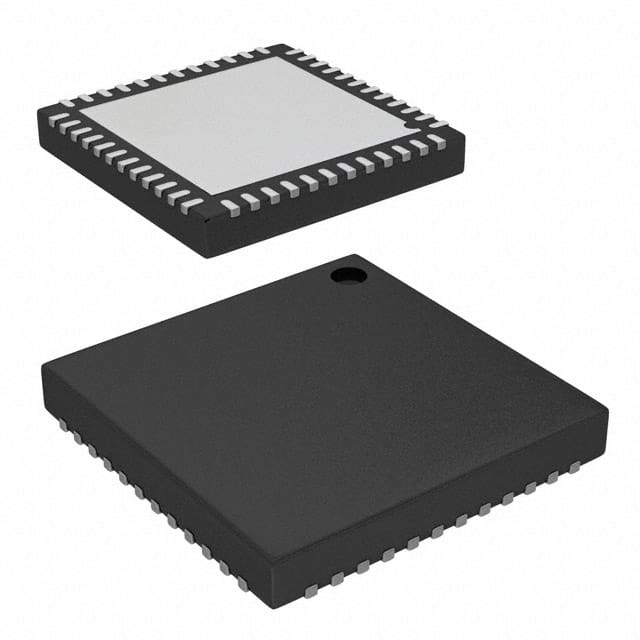
Pin Configuration
For a detailed and complete pin configuration diagram of CY27410FLTXIT, please refer to the product datasheet provided by the manufacturer.
Functional Characteristics
CY27410FLTXIT offers the following functional characteristics:
- Precise frequency generation
- Clock signal distribution
- Phase-locked loop (PLL) functionality
- Programmable output frequencies
- Low jitter performance
Advantages and Disadvantages
Advantages
- High accuracy and stability
- Flexible programmability
- Wide operating temperature range
- Low power consumption
Disadvantages
- Limited frequency range compared to some other models
- Higher cost compared to basic timing components
Applicable Range of Products
CY27410FLTXIT is suitable for a wide range of electronic products, including but not limited to: - Network routers and switches - Wireless communication devices - Audio/video equipment - Industrial control systems - Test and measurement instruments
Working Principles
CY27410FLTXIT operates based on the principles of frequency synthesis and phase-locked loop (PLL) technology. It generates precise clock signals by locking onto an external reference signal and multiplying its frequency using a programmable PLL.
Detailed Application Field Plans
CY27410FLTXIT can be used in various applications, such as: 1. Timing synchronization in telecommunications infrastructure. 2. Clock generation for microprocessors and digital signal processors. 3. Frequency synthesis in wireless communication systems. 4. Clock distribution in data center equipment. 5. Timing control in industrial automation systems.
Detailed Alternative Models
Some alternative models to CY27410FLTXIT include: - CY27411FLTXIT - CY27412FLTXIT - CY27413FLTXIT - CY27414FLTXIT - CY27415FLTXIT
5 Common Technical Questions and Answers
Q: What is the maximum operating frequency of CY27410FLTXIT? A: The maximum operating frequency is 100 MHz.
Q: Can CY27410FLTXIT operate at lower voltages? A: No, the recommended operating voltage is 3.3V.
Q: Does CY27410FLTXIT support multiple output frequencies simultaneously? A: Yes, it has multiple programmable outputs that can generate different frequencies.
Q: Is CY27410FLTXIT compatible with both CMOS and LVCMOS logic levels? A: No, it supports LVCMOS logic levels only.
Q: What is the typical supply current of CY27410FLTXIT? A: The typical supply current is 10 mA.
This encyclopedia entry provides an overview of CY27410FLTXIT, including its basic information, specifications, pin configuration, functional characteristics, advantages and disadvantages, applicable range of products, working principles, detailed application field plans, alternative models, and common technical questions and answers.