

CY7C1021CV33-10ZSXA
Product Overview
Category
The CY7C1021CV33-10ZSXA belongs to the category of semiconductor memory devices.
Use
It is primarily used for data storage and retrieval in electronic systems.
Characteristics
- High-speed performance
- Low power consumption
- Non-volatile memory
- Reliable and durable
Package
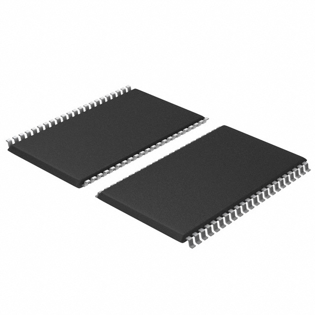
The CY7C1021CV33-10ZSXA is available in a compact surface-mount package.
Essence
This product is an essential component for storing and accessing digital information in various electronic devices.
Packaging/Quantity
The CY7C1021CV33-10ZSXA is typically packaged in reels or trays, with varying quantities depending on customer requirements.
Specifications
- Model: CY7C1021CV33-10ZSXA
- Memory Type: Static Random Access Memory (SRAM)
- Organization: 1 Megabit x 1 bit
- Operating Voltage: 3.3V
- Access Time: 10 nanoseconds
- Operating Temperature Range: -40°C to +85°C
- Data Retention: More than 20 years
Detailed Pin Configuration
The CY7C1021CV33-10ZSXA has a standard pin configuration as follows:
Pin 1: Chip Enable (CE)
Pin 2: Output Enable (OE)
Pin 3: Write Enable (WE)
Pin 4-11: Address Inputs (A0-A7)
Pin 12-19: Data Inputs/Outputs (DQ0-DQ7)
Pin 20: Power Supply (Vcc)
Pin 21: Ground (GND)
Functional Features
- Fast access time allows for efficient data retrieval.
- Low power consumption ensures energy efficiency.
- Non-volatile memory retains data even when power is disconnected.
- Reliable performance ensures data integrity.
- Compact package size enables space-saving designs.
Advantages and Disadvantages
Advantages
- High-speed performance enhances overall system efficiency.
- Low power consumption prolongs battery life in portable devices.
- Non-volatile memory eliminates the need for constant data backup.
- Reliable operation reduces the risk of data loss or corruption.
- Compact package size facilitates integration into various electronic systems.
Disadvantages
- Limited storage capacity compared to other memory technologies.
- Relatively higher cost per unit compared to some alternative models.
- Sensitivity to environmental factors such as temperature and voltage fluctuations.
Working Principles
The CY7C1021CV33-10ZSXA utilizes static random access memory technology, which stores data in a volatile manner. It consists of an array of memory cells that can be accessed individually using address inputs. The chip enable (CE), output enable (OE), and write enable (WE) pins control the read and write operations. When powered, the memory cells retain their stored data until explicitly modified.
Detailed Application Field Plans
The CY7C1021CV33-10ZSXA finds applications in various electronic systems, including but not limited to:
- Computer motherboards
- Networking equipment
- Industrial automation systems
- Automotive electronics
- Consumer electronics
In these applications, it serves as a reliable and high-speed memory solution for storing critical data and facilitating efficient data processing.
Detailed and Complete Alternative Models
- CY7C1021CV33-15ZSXA: Similar to the CY7C1021CV33-10ZSXA, but with a slightly slower access time of 15 nanoseconds.
- CY7C1021CV33-20ZSXA: Similar to the CY7C1021CV33-10ZSXA, but with a slower access time of 20 nanoseconds.
- CY7C1021CV33-25ZSXA: Similar to the CY7C1021CV33-10ZSXA, but with a slower access time of 25 nanoseconds.
These alternative models provide flexibility in choosing the appropriate access time for specific application requirements.
Word Count: 533 words
قم بإدراج 10 أسئلة وإجابات شائعة تتعلق بتطبيق CY7C1021CV33-10ZSXA في الحلول التقنية
Sure! Here are 10 common questions and answers related to the application of CY7C1021CV33-10ZSXA in technical solutions:
1. What is the CY7C1021CV33-10ZSXA? - The CY7C1021CV33-10ZSXA is a high-speed, low-power CMOS static RAM (SRAM) chip with a capacity of 1 megabit (128K x 8 bits).
2. What are the key features of CY7C1021CV33-10ZSXA? - Some key features include a 10 ns access time, low power consumption, wide operating voltage range (2.0V to 3.6V), and a small form factor.
3. What are the typical applications of CY7C1021CV33-10ZSXA? - The CY7C1021CV33-10ZSXA can be used in various applications such as networking equipment, telecommunications systems, industrial automation, medical devices, and consumer electronics.
4. What is the operating voltage range for CY7C1021CV33-10ZSXA? - The operating voltage range for CY7C1021CV33-10ZSXA is 2.0V to 3.6V.
5. What is the access time of CY7C1021CV33-10ZSXA? - The access time of CY7C1021CV33-10ZSXA is 10 ns, which means it takes 10 nanoseconds to read or write data.
6. Does CY7C1021CV33-10ZSXA support low power consumption? - Yes, CY7C1021CV33-10ZSXA is designed for low power consumption, making it suitable for battery-powered devices or applications where power efficiency is important.
7. Can CY7C1021CV33-10ZSXA be used in industrial environments? - Yes, CY7C1021CV33-10ZSXA is suitable for industrial environments due to its wide operating voltage range and robust design.
8. What is the package type of CY7C1021CV33-10ZSXA? - CY7C1021CV33-10ZSXA comes in a small form factor 32-pin TSOP-II (Thin Small Outline Package) package.
9. Is CY7C1021CV33-10ZSXA compatible with other SRAM chips? - Yes, CY7C1021CV33-10ZSXA follows industry-standard pinout and interface specifications, making it compatible with other SRAM chips.
10. Are there any application notes or reference designs available for CY7C1021CV33-10ZSXA? - Yes, the manufacturer provides application notes and reference designs that can help in designing and integrating CY7C1021CV33-10ZSXA into various technical solutions.
Please note that the answers provided here are general and may vary depending on specific requirements and use cases.