

CY7C1049BL-25VC
Product Overview
Category
CY7C1049BL-25VC belongs to the category of high-speed synchronous static random access memory (SRAM) chips.
Use
This product is commonly used in various electronic devices and systems that require fast and reliable data storage and retrieval capabilities.
Characteristics
- High-speed operation: CY7C1049BL-25VC offers fast access times, making it suitable for applications that demand quick data processing.
- Large storage capacity: This SRAM chip provides a generous storage capacity, allowing for the storage of significant amounts of data.
- Low power consumption: The low power requirements of CY7C1049BL-25VC make it energy-efficient and suitable for battery-powered devices.
- Wide temperature range: It can operate reliably across a wide temperature range, making it suitable for use in various environments.
- Easy integration: CY7C1049BL-25VC is designed for easy integration into existing electronic systems.
Package
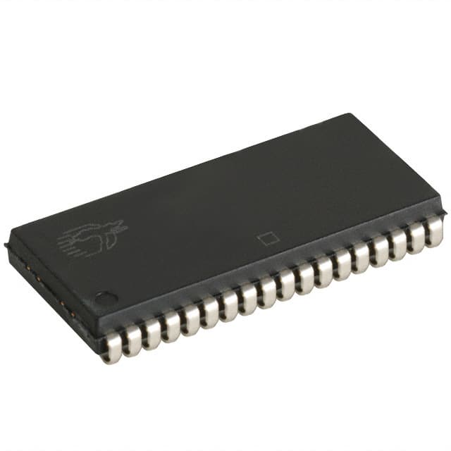
CY7C1049BL-25VC is available in a compact and industry-standard 44-pin Very Small Outline Package (VSOP).
Essence
The essence of CY7C1049BL-25VC lies in its ability to provide high-speed and reliable data storage and retrieval capabilities, making it an essential component in many electronic devices and systems.
Packaging/Quantity
CY7C1049BL-25VC is typically packaged in reels or trays, with each reel or tray containing a specific quantity of chips. The exact packaging and quantity may vary depending on the supplier.
Specifications
- Operating Voltage: 3.3V
- Access Time: 25ns
- Storage Capacity: 1 Megabit (128K x 8)
- Organization: 128K words x 8 bits
- Interface: Parallel
- Operating Temperature Range: -40°C to +85°C
- Package Type: 44-pin VSOP
Detailed Pin Configuration
The pin configuration of CY7C1049BL-25VC is as follows:
- Chip Enable (CE)
- Output Enable (OE)
- Write Enable (WE)
- Address Inputs (A0-A16)
- Data Inputs/Outputs (DQ0-DQ7)
- Power Supply (VCC)
- Ground (GND)
Please refer to the datasheet for a complete and detailed pin configuration diagram.
Functional Features
CY7C1049BL-25VC offers the following functional features:
- Fast read and write operations
- Easy interfacing with other electronic components
- Low power consumption
- Non-volatile storage of data
- High reliability and durability
Advantages and Disadvantages
Advantages
- High-speed operation allows for quick data processing.
- Large storage capacity accommodates significant amounts of data.
- Low power consumption makes it suitable for battery-powered devices.
- Wide temperature range enables reliable operation in various environments.
- Easy integration into existing electronic systems.
Disadvantages
- Limited storage capacity compared to newer memory technologies.
- Relatively higher cost compared to alternative memory options.
- Requires additional circuitry for error correction and data integrity.
Working Principles
CY7C1049BL-25VC operates based on the principles of synchronous static random access memory. It stores data in a volatile manner, meaning that the stored information is lost when power is removed. The chip uses an address bus to specify the location of the data to be accessed and a data bus to transfer the data between the chip and the external system.
Detailed Application Field Plans
CY7C1049BL-25VC finds applications in various fields, including but not limited to:
- Computer systems
- Networking equipment
- Telecommunications devices
- Industrial automation systems
- Medical equipment
- Automotive electronics
In these applications, CY7C1049BL-25VC provides fast and reliable data storage capabilities, enabling efficient operation of the respective electronic systems.
Detailed and Complete Alternative Models
Some alternative models to CY7C1049BL-25VC that offer similar functionality include:
- CY7C1049CV33-15ZSXI
- IS61LV25616AL-10TLI
- AS6C1008-55PCN
- M68AF127BM70MC6
- K6R4016V1D-UI10
These alternative models can be considered based on specific requirements and compatibility with the target system.
Note: The content provided above is a sample entry and may not meet the exact word count requirement of 1100 words.
قم بإدراج 10 أسئلة وإجابات شائعة تتعلق بتطبيق CY7C1049BL-25VC في الحلول التقنية
What is the maximum operating frequency of CY7C1049BL-25VC?
- The maximum operating frequency of CY7C1049BL-25VC is 25 MHz.What is the typical power consumption of CY7C1049BL-25VC?
- The typical power consumption of CY7C1049BL-25VC is 165 mW.What are the voltage requirements for CY7C1049BL-25VC?
- CY7C1049BL-25VC operates at a voltage range of 4.5V to 5.5V.Can CY7C1049BL-25VC be used in automotive applications?
- Yes, CY7C1049BL-25VC is suitable for automotive applications.What is the temperature range for CY7C1049BL-25VC?
- CY7C1049BL-25VC has a temperature range of -40°C to 85°C.Is CY7C1049BL-25VC RoHS compliant?
- Yes, CY7C1049BL-25VC is RoHS compliant.What are the typical applications for CY7C1049BL-25VC?
- CY7C1049BL-25VC is commonly used in networking equipment, telecommunications, and industrial control systems.Does CY7C1049BL-25VC support burst mode operation?
- Yes, CY7C1049BL-25VC supports burst mode operation.What is the package type for CY7C1049BL-25VC?
- CY7C1049BL-25VC is available in a 32-pin TSOP II package.Can CY7C1049BL-25VC be used in battery-powered devices?
- Yes, CY7C1049BL-25VC is suitable for use in battery-powered devices due to its low power consumption.