

CY7C1061G30-10ZSXIT
Product Overview
Category
The CY7C1061G30-10ZSXIT belongs to the category of synchronous static random access memory (SRAM) chips.
Use
This product is primarily used in electronic devices and systems that require high-speed read and write operations, such as computers, servers, networking equipment, and telecommunications devices.
Characteristics
- High-speed operation: The CY7C1061G30-10ZSXIT offers fast access times, allowing for efficient data retrieval and storage.
- Low power consumption: This SRAM chip is designed to minimize power usage, making it suitable for battery-powered devices.
- High density: With a capacity of 1 megabit (128K x 8 bits), this chip provides ample storage space for various applications.
- Wide voltage range: The CY7C1061G30-10ZSXIT operates within a voltage range of 2.3V to 3.6V, ensuring compatibility with different system requirements.
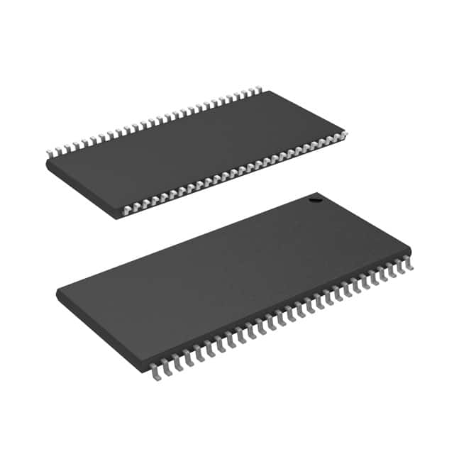
Package
The CY7C1061G30-10ZSXIT is available in a small outline integrated circuit (SOIC) package, which facilitates easy integration into circuit boards.
Essence
This SRAM chip serves as a reliable and high-performance memory component, enabling efficient data storage and retrieval in electronic systems.
Packaging/Quantity
The CY7C1061G30-10ZSXIT is typically packaged in reels, containing a quantity of 2500 units per reel.
Specifications
- Organization: 128K x 8 bits
- Access Time: 10 ns
- Operating Voltage Range: 2.3V to 3.6V
- Standby Current: 5 µA (typical)
- Operating Temperature Range: -40°C to +85°C
- Package Type: SOIC
Detailed Pin Configuration
The CY7C1061G30-10ZSXIT has a total of 32 pins, which are assigned specific functions as follows:
- A0 - Address Input
- A1 - Address Input
- A2 - Address Input
- A3 - Address Input
- A4 - Address Input
- A5 - Address Input
- A6 - Address Input
- A7 - Address Input
- VCC - Power Supply
- A8 - Address Input
- A9 - Address Input
- A10 - Address Input
- A11 - Address Input
- A12 - Address Input
- A13 - Address Input
- A14 - Address Input
- A15 - Address Input
- /WE - Write Enable Input
- /OE - Output Enable Input
- I/O0 - Data Input/Output
- I/O1 - Data Input/Output
- I/O2 - Data Input/Output
- I/O3 - Data Input/Output
- I/O4 - Data Input/Output
- I/O5 - Data Input/Output
- I/O6 - Data Input/Output
- I/O7 - Data Input/Output
- GND - Ground
- NC - No Connection
- NC - No Connection
- NC - No Connection
- NC - No Connection
Functional Features
- High-speed operation allows for quick data access and transfer.
- Low power consumption ensures energy efficiency in electronic systems.
- Reliable performance and durability make it suitable for various applications.
- Wide voltage range compatibility enables integration into different system designs.
Advantages and Disadvantages
Advantages
- Fast access times enhance overall system performance.
- Low power consumption prolongs battery life in portable devices.
- High density provides ample storage capacity for data-intensive applications.
- Wide voltage range compatibility allows for versatile integration.
Disadvantages
- Limited storage capacity compared to higher-capacity memory chips.
- Relatively higher cost per unit compared to lower-density alternatives.
- Requires careful handling and proper ESD precautions during installation.
Working Principles
The CY7C1061G30-10ZSXIT operates based on the principles of synchronous static random access memory. It stores and retrieves data using a combination of address inputs, write enable and output enable signals, and data input/output lines. The chip's internal circuitry ensures reliable and efficient data transfer between the memory cells and the external system.
Detailed Application Field Plans
The CY7C1061G30-10ZSXIT finds application in various electronic systems that require high-speed and reliable data storage and retrieval. Some specific application fields include:
- Computer systems: Used as cache memory or main memory in desktops, laptops, and servers.
- Networking equipment: Enables fast packet buffering and data processing in routers and
قم بإدراج 10 أسئلة وإجابات شائعة تتعلق بتطبيق CY7C1061G30-10ZSXIT في الحلول التقنية
Sure! Here are 10 common questions and answers related to the application of CY7C1061G30-10ZSXIT in technical solutions:
1. What is CY7C1061G30-10ZSXIT? CY7C1061G30-10ZSXIT is a specific model of synchronous SRAM (Static Random Access Memory) chip manufactured by Cypress Semiconductor. It has a capacity of 1 Megabit (128K x 8) and operates at a speed of 10 nanoseconds.
2. What are the typical applications of CY7C1061G30-10ZSXIT? CY7C1061G30-10ZSXIT is commonly used in various technical solutions that require fast and reliable memory storage, such as networking equipment, telecommunications systems, industrial automation, and embedded systems.
3. What is the voltage requirement for CY7C1061G30-10ZSXIT? CY7C1061G30-10ZSXIT operates at a voltage range of 4.5V to 5.5V.
4. What is the operating temperature range for CY7C1061G30-10ZSXIT? CY7C1061G30-10ZSXIT can operate within a temperature range of -40°C to +85°C.
5. Does CY7C1061G30-10ZSXIT support multiple read/write operations simultaneously? No, CY7C1061G30-10ZSXIT is a synchronous SRAM and does not support simultaneous read/write operations. It follows a synchronous protocol where read and write operations are performed sequentially.
6. Can CY7C1061G30-10ZSXIT be used in battery-powered devices? Yes, CY7C1061G30-10ZSXIT can be used in battery-powered devices as it operates at a relatively low voltage and has low power consumption.
7. Does CY7C1061G30-10ZSXIT have any built-in error correction capabilities? No, CY7C1061G30-10ZSXIT does not have built-in error correction capabilities. It is a standard synchronous SRAM without error correction features.
8. Can CY7C1061G30-10ZSXIT be used in high-speed data processing applications? Yes, CY7C1061G30-10ZSXIT has a fast access time of 10 nanoseconds, making it suitable for high-speed data processing applications that require quick memory access.
9. What is the package type for CY7C1061G30-10ZSXIT? CY7C1061G30-10ZSXIT comes in a 32-pin TSOP (Thin Small Outline Package) form factor.
10. Is CY7C1061G30-10ZSXIT compatible with other memory chips or microcontrollers? Yes, CY7C1061G30-10ZSXIT follows industry-standard protocols and can be easily interfaced with other memory chips or microcontrollers that support synchronous SRAM interfaces.