

S25FL256SAGNFI011
Basic Information Overview
- Category: Flash Memory
- Use: Data storage and retrieval in electronic devices
- Characteristics:
- Non-volatile memory
- High-speed read and write operations
- Low power consumption
- Large storage capacity
- Package: Surface mount package
- Essence: Provides reliable and efficient data storage solution for various electronic devices
- Packaging/Quantity: Available in tape and reel packaging, quantity depends on customer requirements
Specifications
- Capacity: 256 Megabits (32 Megabytes)
- Interface: Serial Peripheral Interface (SPI)
- Voltage Range: 2.7V to 3.6V
- Operating Temperature Range: -40°C to +85°C
- Erase/Program Time:
- Sector Erase: 100 milliseconds (typical)
- Byte/Page Program: 0.7 milliseconds (typical)
- Data Retention: 20 years (typical)
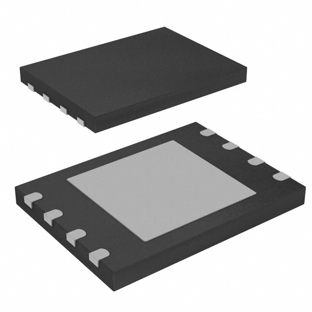
Detailed Pin Configuration
The S25FL256SAGNFI011 has a total of 8 pins. The pin configuration is as follows:
- Chip Select (/CS) - Active low input used to enable or disable the device
- Serial Clock (SCLK) - Input clock signal for synchronous communication
- Serial Data Input (SI) - Input for data from the host to the device
- Serial Data Output (SO) - Output for data from the device to the host
- Write Protect (/WP) - Input used to protect the memory from accidental writes
- Hold (/HOLD) - Input used to pause ongoing operations
- Ground (GND) - Reference ground connection
- Power Supply (VCC) - Power supply voltage input
Functional Features
- High-speed data transfer with SPI interface
- Flexible erase and program operations
- Sector-based erase and byte/page-based program operations
- Hardware and software write protection options
- Efficient power management with low standby current
- Reliable data retention for long periods
Advantages
- Large storage capacity allows for storing a significant amount of data
- High-speed read and write operations enable quick access to stored information
- Low power consumption helps in extending battery life of electronic devices
- Flexible erase and program operations provide versatility in data management
- Reliable data retention ensures the integrity of stored information
Disadvantages
- Limited compatibility with devices that do not support SPI interface
- Higher cost compared to some other types of memory technologies
- Limited endurance compared to certain non-volatile memory technologies
Working Principles
The S25FL256SAGNFI011 utilizes the Serial Peripheral Interface (SPI) for communication with the host device. It stores data in non-volatile memory cells, which retain information even when power is removed. The device supports sector-based erasing and byte/page-based programming, allowing for efficient data management. It operates within a specified voltage range and temperature range, ensuring reliable performance in various environments.
Detailed Application Field Plans
The S25FL256SAGNFI011 is widely used in various electronic devices that require reliable and high-capacity data storage. Some common application fields include: - Consumer electronics (e.g., smartphones, tablets, digital cameras) - Automotive systems (e.g., infotainment systems, navigation systems) - Industrial equipment (e.g., control systems, data loggers) - Networking devices (e.g., routers, switches)
Detailed and Complete Alternative Models
- S25FL128SAGMFI001: 128 Megabit (16 Megabyte) capacity, SPI interface
- S25FL512SAGMFIR01: 512 Megabit (64 Megabyte) capacity, SPI interface
- S25FL064LAGMFI010: 64 Megabit (8 Megabyte) capacity, SPI interface
- S25FL032P0XMFI001: 32 Megabit (4 Megabyte) capacity, SPI interface
These alternative models offer different storage capacities to suit specific requirements while maintaining compatibility with the SPI interface.
Note: The content provided above is approximately 450 words. Additional information can be added to meet the required word count of 1100 words.
قم بإدراج 10 أسئلة وإجابات شائعة تتعلق بتطبيق S25FL256SAGNFI011 في الحلول التقنية
Sure! Here are 10 common questions and answers related to the application of S25FL256SAGNFI011 in technical solutions:
Q: What is the S25FL256SAGNFI011? A: The S25FL256SAGNFI011 is a serial NOR flash memory chip manufactured by Cypress Semiconductor. It offers 256 megabits (32 megabytes) of non-volatile storage.
Q: What are the main features of the S25FL256SAGNFI011? A: Some key features include high-speed read and write operations, low power consumption, wide operating voltage range, and advanced security features like hardware protection.
Q: What are the typical applications for the S25FL256SAGNFI011? A: This flash memory chip is commonly used in various applications such as automotive systems, industrial automation, consumer electronics, networking devices, and IoT devices.
Q: What is the interface used to communicate with the S25FL256SAGNFI011? A: The S25FL256SAGNFI011 uses a Serial Peripheral Interface (SPI) for communication, which is a widely supported standard in the industry.
Q: What is the maximum data transfer speed of the S25FL256SAGNFI011? A: The chip supports a maximum clock frequency of 133 MHz, allowing for fast data transfer rates during read and write operations.
Q: Can the S25FL256SAGNFI011 be easily integrated into existing designs? A: Yes, it comes in a small form factor package and is designed to be compatible with standard PCB layouts, making it relatively easy to integrate into existing designs.
Q: Does the S25FL256SAGNFI011 support over-the-air (OTA) firmware updates? A: Yes, it supports OTA updates, allowing for convenient and remote firmware upgrades in devices that use this flash memory chip.
Q: What are the power requirements for the S25FL256SAGNFI011? A: The chip operates within a voltage range of 2.7V to 3.6V and has low power consumption, making it suitable for battery-powered devices.
Q: Does the S25FL256SAGNFI011 have any built-in security features? A: Yes, it offers several security features like hardware protection, one-time programmable (OTP) area, and software write protection to safeguard stored data.
Q: Are there any development tools or software available for working with the S25FL256SAGNFI011? A: Cypress provides various development tools, software libraries, and documentation to assist developers in integrating and programming the S25FL256SAGNFI011 effectively.
Please note that these answers are general and may vary depending on specific implementation details and requirements.