

Encyclopedia Entry: 74AUP1G125FW5-7
Product Overview
Category
The 74AUP1G125FW5-7 belongs to the category of integrated circuits (ICs), specifically a single bus buffer gate.
Use
This IC is commonly used in digital logic circuits to provide buffering and signal amplification for a single input/output line.
Characteristics
- Low power consumption
- High-speed operation
- Wide operating voltage range
- Small package size
- RoHS compliant
Package
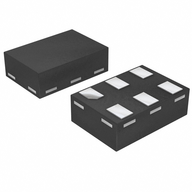
The 74AUP1G125FW5-7 is available in a small SOT353 package, which is a surface-mount package with three leads.
Essence
The essence of this product lies in its ability to amplify and buffer digital signals, ensuring reliable transmission between different components of a digital circuit.
Packaging/Quantity
The 74AUP1G125FW5-7 is typically packaged in reels or tubes, containing a quantity of 3000 units per reel/tube.
Specifications
- Supply Voltage Range: 0.8V to 3.6V
- Input Voltage Range: -0.5V to VCC + 0.5V
- Output Voltage Range: -0.5V to VCC + 0.5V
- Operating Temperature Range: -40°C to +85°C
- Maximum Propagation Delay: 2.5ns at 3.3V supply voltage
Detailed Pin Configuration
The 74AUP1G125FW5-7 has the following pin configuration:
____
   Y --|    |-- VCC
   A --|    |-- GND
   OE --|    |-- A
       ------
Functional Features
- Single bus buffer gate with tri-state output
- Provides signal buffering and amplification
- Enables bidirectional data flow
- Output can be disabled using the OE (Output Enable) pin
Advantages and Disadvantages
Advantages
- Low power consumption makes it suitable for battery-powered devices
- High-speed operation allows for efficient data transmission
- Wide operating voltage range provides flexibility in different applications
- Small package size saves board space
Disadvantages
- Limited number of input/output lines supported
- May not be suitable for high-current applications
Working Principles
The 74AUP1G125FW5-7 operates by receiving a digital signal at the input pin (A), amplifying and buffering it, and then transmitting the amplified signal to the output pin (Y). The tri-state output feature allows the output to be disabled when the OE pin is set to a specific logic level.
Detailed Application Field Plans
The 74AUP1G125FW5-7 finds application in various digital systems, including but not limited to: - Microcontrollers - Communication devices - Data storage systems - Consumer electronics - Automotive electronics
Detailed and Complete Alternative Models
Some alternative models that serve similar functions to the 74AUP1G125FW5-7 include: - SN74LVC1G125DBVR - MC74VHC1GT125DF1G - TC7SZ125FU
These alternatives offer comparable features and performance, providing options for designers based on specific requirements.
In conclusion, the 74AUP1G125FW5-7 is a versatile single bus buffer gate IC with low power consumption, high-speed operation, and a wide operating voltage range. Its small package size and tri-state output make it suitable for various digital applications. Designers can also consider alternative models based on their specific needs.
قم بإدراج 10 أسئلة وإجابات شائعة تتعلق بتطبيق 74AUP1G125FW5-7 في الحلول التقنية
Sure! Here are 10 common questions and answers related to the application of 74AUP1G125FW5-7 in technical solutions:
Q1: What is the 74AUP1G125FW5-7? A1: The 74AUP1G125FW5-7 is a single bus buffer gate with 3-state output, designed for low-power applications.
Q2: What is the operating voltage range of the 74AUP1G125FW5-7? A2: The operating voltage range is from 0.8V to 3.6V.
Q3: What is the maximum output current of the 74AUP1G125FW5-7? A3: The maximum output current is 32mA.
Q4: Can the 74AUP1G125FW5-7 be used as a level shifter? A4: Yes, the 74AUP1G125FW5-7 can be used as a level shifter between different voltage domains.
Q5: What is the propagation delay of the 74AUP1G125FW5-7? A5: The propagation delay is typically 2.5ns.
Q6: Can the 74AUP1G125FW5-7 drive capacitive loads? A6: Yes, the 74AUP1G125FW5-7 can drive capacitive loads up to 50pF.
Q7: Is the 74AUP1G125FW5-7 compatible with other logic families? A7: Yes, the 74AUP1G125FW5-7 is compatible with both CMOS and TTL logic families.
Q8: Does the 74AUP1G125FW5-7 have internal pull-up or pull-down resistors? A8: No, the 74AUP1G125FW5-7 does not have internal pull-up or pull-down resistors.
Q9: Can the 74AUP1G125FW5-7 be used in high-speed applications? A9: Yes, the 74AUP1G125FW5-7 can be used in high-speed applications with a maximum frequency of 500MHz.
Q10: What is the package type of the 74AUP1G125FW5-7? A10: The 74AUP1G125FW5-7 is available in a SOT353 package.
Please note that these answers are based on general information about the 74AUP1G125FW5-7 and may vary depending on specific application requirements.