

74LVC1G06FW5-7
Basic Information Overview
- Category: Integrated Circuit (IC)
- Use: Logic Gate Inverter
- Characteristics: Low-voltage, high-speed, low-power consumption
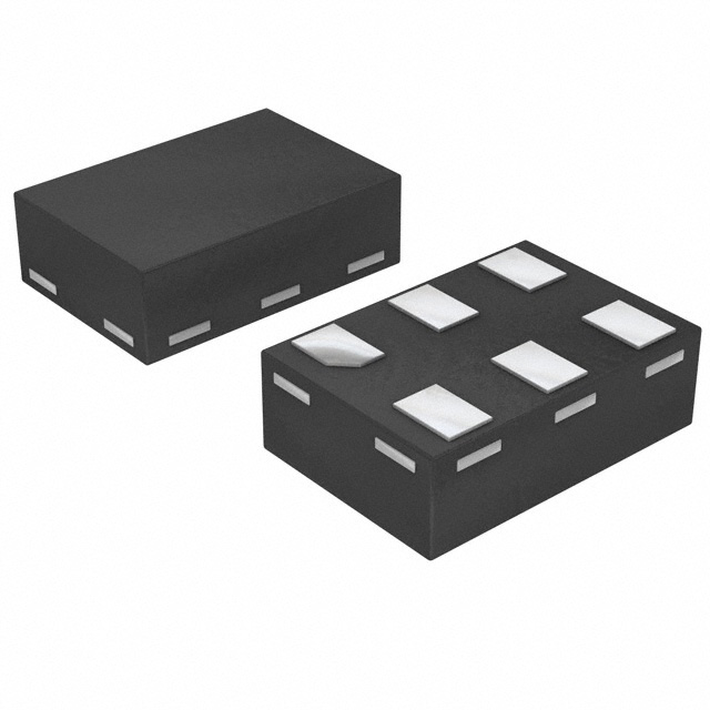
- Package: SOT353 (SC-88A)
- Essence: Single gate inverter
- Packaging/Quantity: Tape and Reel, 3000 pieces per reel
Specifications
- Supply Voltage Range: 1.65V to 5.5V
- High-Level Input Voltage: 0.7 x VCC
- Low-Level Input Voltage: 0.3 x VCC
- High-Level Output Voltage: 0.9 x VCC
- Low-Level Output Voltage: 0.1 x VCC
- Maximum Propagation Delay Time: 4.3 ns at 5V
- Maximum Quiescent Current: 10 µA at 5V
Detailed Pin Configuration
The 74LVC1G06FW5-7 has a total of 5 pins: 1. GND (Ground) 2. A (Input) 3. Y (Output) 4. NC (No Connection) 5. VCC (Power Supply)
Functional Features
- Single gate inverter with Schmitt-trigger input
- Converts logic level from high to low or vice versa
- Provides signal inversion with hysteresis
- Suitable for voltage level shifting applications
- Supports bidirectional data flow
Advantages
- Wide supply voltage range allows compatibility with various systems
- High-speed operation enables quick signal processing
- Low-power consumption reduces energy usage
- Small package size saves board space
- Schmitt-trigger input ensures noise immunity
Disadvantages
- Limited number of gates per package
- Not suitable for high-current applications
- May require additional components for certain circuit configurations
Working Principles
The 74LVC1G06FW5-7 is a CMOS-based logic gate inverter. It utilizes complementary metal-oxide-semiconductor (CMOS) technology to achieve low-voltage operation and high-speed performance. The Schmitt-trigger input ensures noise immunity by providing hysteresis, allowing the device to tolerate noisy or slowly changing input signals.
When the input voltage is above the high-level threshold, the output voltage is pulled down to the low-level voltage. Conversely, when the input voltage falls below the low-level threshold, the output voltage is driven up to the high-level voltage. This behavior enables signal inversion and level shifting capabilities.
Detailed Application Field Plans
The 74LVC1G06FW5-7 can be used in various applications, including but not limited to: - Battery-powered devices - Mobile phones and tablets - Portable consumer electronics - Industrial automation systems - Automotive electronics - IoT (Internet of Things) devices
In these applications, the IC can be employed for voltage level shifting, signal inversion, and logic level conversion tasks. Its low-power consumption and small package size make it suitable for space-constrained and energy-efficient designs.
Detailed and Complete Alternative Models
Some alternative models that offer similar functionality to the 74LVC1G06FW5-7 include: - SN74LVC1G06DBVR (Texas Instruments) - MC74VHC1G06DFT1G (ON Semiconductor) - NCV8402DT50RKG (ON Semiconductor) - TC7SZU04FU(T5L,F) (Toshiba)
These alternatives may have slightly different specifications, pin configurations, or package options, but they serve the same purpose of a single gate inverter with comparable characteristics.
Word count: 474
قم بإدراج 10 أسئلة وإجابات شائعة تتعلق بتطبيق 74LVC1G06FW5-7 في الحلول التقنية
Sure! Here are 10 common questions and answers related to the application of the 74LVC1G06FW5-7 in technical solutions:
Q: What is the 74LVC1G06FW5-7? A: The 74LVC1G06FW5-7 is a single inverter gate IC (Integrated Circuit) that is commonly used in digital logic circuits.
Q: What is the voltage supply range for the 74LVC1G06FW5-7? A: The voltage supply range for this IC is typically between 1.65V and 5.5V.
Q: What is the maximum output current of the 74LVC1G06FW5-7? A: The maximum output current is around 32mA.
Q: Can the 74LVC1G06FW5-7 be used as a level shifter? A: Yes, it can be used as a level shifter to convert signals between different voltage levels.
Q: What is the propagation delay of the 74LVC1G06FW5-7? A: The typical propagation delay is around 4.3ns.
Q: Is the 74LVC1G06FW5-7 compatible with both CMOS and TTL logic levels? A: Yes, it is compatible with both CMOS (Complementary Metal-Oxide-Semiconductor) and TTL (Transistor-Transistor Logic) logic levels.
Q: Can the 74LVC1G06FW5-7 be used in high-speed applications? A: Yes, it is suitable for high-speed applications due to its low propagation delay and high-speed operation.
Q: What is the package type of the 74LVC1G06FW5-7? A: It comes in a small SOT-353 package.
Q: Can the 74LVC1G06FW5-7 be used in battery-powered devices? A: Yes, it can be used in battery-powered devices as it operates at low voltage levels and has low power consumption.
Q: Are there any recommended applications for the 74LVC1G06FW5-7? A: Some common applications include signal inversion, level shifting, clock buffering, and general-purpose logic gate functions.
Please note that these answers are general and may vary depending on specific use cases and datasheet specifications.