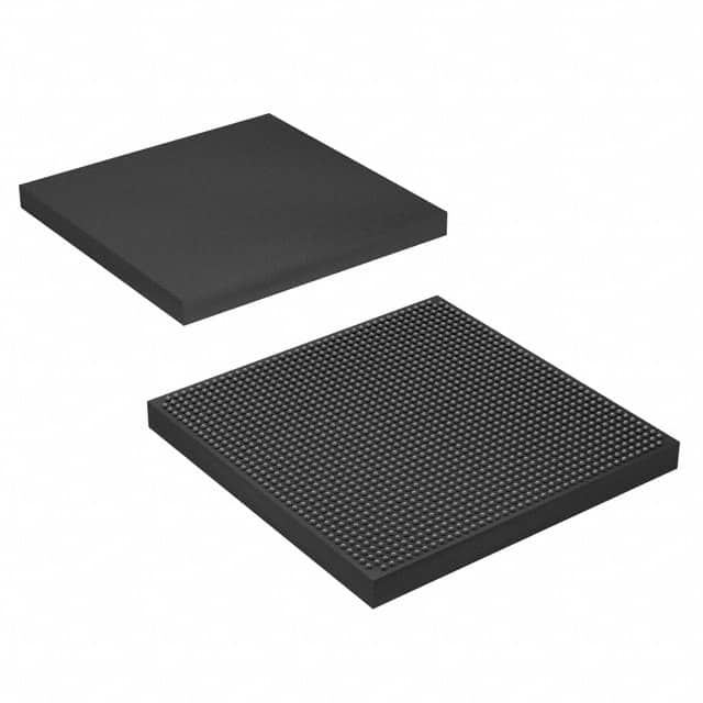
5SGSMD5K2F40C1
Basic Information Overview
- Category: Integrated Circuit (IC)
- Use: Digital Signal Processing (DSP)
- Characteristics: High-performance, low-power consumption
- Package: BGA (Ball Grid Array)
- Essence: Field Programmable Gate Array (FPGA)
- Packaging/Quantity: Single unit
Specifications
- Manufacturer: Intel Corporation
- Family: Stratix V
- Device: 5SGSMD5K2F40C1
- Logic Elements: 462,000
- Embedded Memory: 25,920 Kbits
- DSP Blocks: 3,888
- Maximum User I/O Pins: 1,280
- Operating Voltage: 1.0V
- Operating Temperature: -40°C to 100°C
Detailed Pin Configuration
The 5SGSMD5K2F40C1 has a complex pin configuration with multiple pins dedicated to various functions. The detailed pin configuration can be found in the manufacturer's datasheet.
Functional Features
- High-speed data processing capabilities
- Configurable logic elements for custom designs
- On-chip memory for efficient data storage
- Dedicated DSP blocks for signal processing tasks
- Support for various communication protocols
- Low power consumption for energy-efficient operation
Advantages and Disadvantages
Advantages: - Versatile and flexible design options - High-performance computing capabilities - Efficient utilization of resources - Wide range of supported applications
Disadvantages: - Complex programming and configuration process - Limited availability of alternative models - Higher cost compared to general-purpose microcontrollers
Working Principles
The 5SGSMD5K2F40C1 is based on FPGA technology, which allows users to configure the device according to their specific requirements. It consists of configurable logic elements, embedded memory, and dedicated DSP blocks. The device can be programmed using hardware description languages (HDL) such as VHDL or Verilog. Once programmed, the FPGA executes the desired logic operations and performs signal processing tasks.
Detailed Application Field Plans
The 5SGSMD5K2F40C1 finds applications in various fields, including: - Telecommunications: Signal processing, data compression, encryption/decryption - Aerospace and Defense: Radar systems, image processing, communication systems - Industrial Automation: Control systems, robotics, machine vision - Medical Imaging: Image reconstruction, real-time processing - High-Performance Computing: Cryptography, simulation, scientific computing
Detailed and Complete Alternative Models
While the 5SGSMD5K2F40C1 is a specific model within the Stratix V family, there are alternative models available from Intel Corporation and other FPGA manufacturers. Some alternative models within the same family include: - 5SGSMD5K2F40I2 - 5SGSMD5K2F40H2 - 5SGSMD5K2F40E2
It is recommended to refer to the manufacturer's website or consult with an authorized distributor for a complete list of alternative models.
Word count: 285
قم بإدراج 10 أسئلة وإجابات شائعة تتعلق بتطبيق 5SGSMD5K2F40C1 في الحلول التقنية
Sure! Here are 10 common questions and answers related to the application of 5SGSMD5K2F40C1 in technical solutions:
Q1: What is the 5SGSMD5K2F40C1 FPGA used for? A1: The 5SGSMD5K2F40C1 FPGA is commonly used for high-performance applications such as data centers, networking, telecommunications, and industrial automation.
Q2: What is the maximum operating frequency of the 5SGSMD5K2F40C1 FPGA? A2: The maximum operating frequency of the 5SGSMD5K2F40C1 FPGA is typically around 500 MHz, but it can vary depending on the specific design and implementation.
Q3: How many logic elements (LEs) does the 5SGSMD5K2F40C1 FPGA have? A3: The 5SGSMD5K2F40C1 FPGA has approximately 220,000 logic elements (LEs), which can be used to implement various digital circuits and functions.
Q4: Can the 5SGSMD5K2F40C1 FPGA support multiple communication protocols? A4: Yes, the 5SGSMD5K2F40C1 FPGA supports multiple communication protocols such as PCIe, Ethernet, USB, and DDR3/DDR4 memory interfaces, making it versatile for different applications.
Q5: What is the power consumption of the 5SGSMD5K2F40C1 FPGA? A5: The power consumption of the 5SGSMD5K2F40C1 FPGA depends on the specific design and usage scenario. It typically ranges from a few watts to tens of watts.
Q6: Can the 5SGSMD5K2F40C1 FPGA be reprogrammed? A6: Yes, the 5SGSMD5K2F40C1 FPGA can be reprogrammed multiple times, allowing for flexibility in design iterations and updates.
Q7: Does the 5SGSMD5K2F40C1 FPGA have built-in security features? A7: Yes, the 5SGSMD5K2F40C1 FPGA provides built-in security features such as secure boot, encrypted configuration bitstreams, and physical tamper detection mechanisms.
Q8: What development tools are available for programming the 5SGSMD5K2F40C1 FPGA? A8: The 5SGSMD5K2F40C1 FPGA can be programmed using Intel Quartus Prime software, which provides a comprehensive suite of design and verification tools.
Q9: Can the 5SGSMD5K2F40C1 FPGA interface with external devices? A9: Yes, the 5SGSMD5K2F40C1 FPGA supports various I/O standards and can interface with external devices such as sensors, displays, and other peripherals.
Q10: Are there any reference designs or application notes available for the 5SGSMD5K2F40C1 FPGA? A10: Yes, Intel (formerly Altera) provides a wide range of reference designs, application notes, and documentation to help users get started with the 5SGSMD5K2F40C1 FPGA and implement specific functionalities.
Please note that the answers provided here are general and may vary depending on the specific requirements and use cases.


