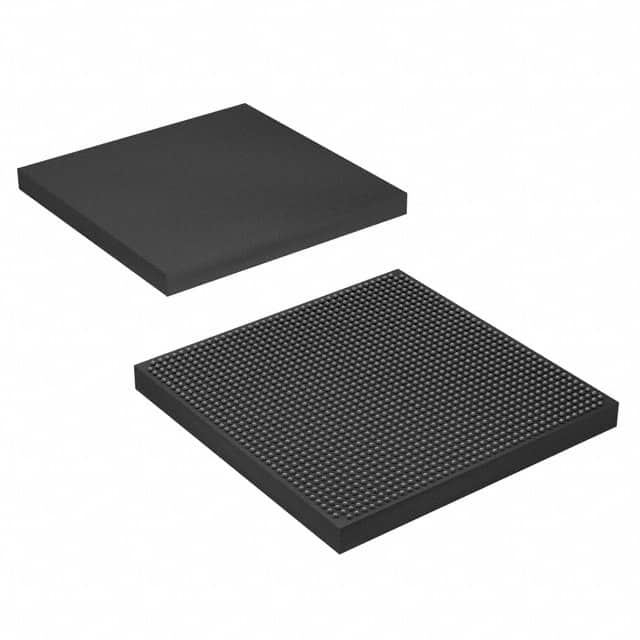
5SGXEA5K3F40C2LN
Basic Information Overview
- Category: Integrated Circuit (IC)
- Use: Programmable Logic Device (PLD)
- Characteristics: High-performance, low-power consumption, high-density
- Package: BGA (Ball Grid Array)
- Essence: FPGA (Field-Programmable Gate Array)
- Packaging/Quantity: Tray, 1 piece
Specifications
- Family: Stratix V
- Device: 5SGXEA5K3F40C2LN
- Logic Elements: 462,000
- Embedded Memory: 13,824 Kbits
- DSP Blocks: 1,288
- Maximum User I/O Pins: 1,040
- Operating Voltage: 1.0V
- Speed Grade: -2
- Temperature Range: -40°C to +100°C
Detailed Pin Configuration
The 5SGXEA5K3F40C2LN has a complex pin configuration with various input/output pins, power supply pins, and configuration pins. The detailed pin configuration can be found in the datasheet provided by the manufacturer.
Functional Features
- High-performance processing capabilities
- Flexible and reprogrammable design
- Low-power consumption
- High-density integration
- Support for various communication protocols
- On-chip memory resources
- Built-in digital signal processing capabilities
Advantages
- Versatile and adaptable for different applications
- Allows for rapid prototyping and development
- Offers high-speed data processing
- Enables complex algorithms and computations
- Provides flexibility for system upgrades and modifications
Disadvantages
- Complexity may require specialized knowledge for optimal utilization
- Higher cost compared to fixed-function integrated circuits
- Limited analog functionality compared to dedicated analog ICs
Working Principles
The 5SGXEA5K3F40C2LN is a programmable logic device based on FPGA technology. It consists of an array of configurable logic blocks interconnected through programmable interconnects. The device can be programmed to implement various digital circuits and functions by configuring the interconnections and logic elements.
Detailed Application Field Plans
The 5SGXEA5K3F40C2LN is widely used in applications that require high-performance digital processing, such as: - Telecommunications and networking equipment - Industrial automation and control systems - High-speed data processing and analysis - Video and image processing - Aerospace and defense systems - Scientific research and development
Detailed and Complete Alternative Models
- 5SGXEA7N2F45C2LN
- 5SGXEA9H2F35C2LN
- 5SGXEA3H2F35C2LN
- 5SGXEA5H2F35C2LN
- 5SGXEA7H2F35C2LN
These alternative models offer similar functionality and performance but may have different capacity, speed grade, or package options.
Note: The above information is provided as a general overview. For detailed technical specifications and pin configurations, please refer to the manufacturer's datasheet.
قم بإدراج 10 أسئلة وإجابات شائعة تتعلق بتطبيق 5SGXEA5K3F40C2LN في الحلول التقنية
Sure! Here are 10 common questions and answers related to the application of 5SGXEA5K3F40C2LN in technical solutions:
Q: What is the 5SGXEA5K3F40C2LN FPGA used for? A: The 5SGXEA5K3F40C2LN is a Field-Programmable Gate Array (FPGA) that can be used for various applications such as high-performance computing, networking, and signal processing.
Q: What are the key features of the 5SGXEA5K3F40C2LN FPGA? A: Some key features of this FPGA include a large number of logic elements, high-speed transceivers, embedded memory blocks, and support for various communication protocols.
Q: Can the 5SGXEA5K3F40C2LN FPGA be used for real-time video processing? A: Yes, the FPGA's high-performance capabilities make it suitable for real-time video processing applications like video encoding, decoding, and image recognition.
Q: Is the 5SGXEA5K3F40C2LN FPGA suitable for high-bandwidth networking applications? A: Absolutely! This FPGA offers high-speed transceivers and support for various networking protocols, making it ideal for high-bandwidth networking applications.
Q: Can the 5SGXEA5K3F40C2LN FPGA be used for implementing cryptographic algorithms? A: Yes, the FPGA's flexible architecture allows for the implementation of cryptographic algorithms, providing hardware acceleration for encryption and decryption tasks.
Q: Does the 5SGXEA5K3F40C2LN FPGA support PCIe connectivity? A: Yes, this FPGA supports PCIe (Peripheral Component Interconnect Express) connectivity, enabling easy integration with other PCIe devices in a system.
Q: Can the 5SGXEA5K3F40C2LN FPGA be used for high-performance computing applications? A: Absolutely! With its large number of logic elements and high-speed transceivers, this FPGA is well-suited for demanding high-performance computing tasks.
Q: Does the 5SGXEA5K3F40C2LN FPGA support multiple voltage levels? A: Yes, this FPGA supports multiple voltage levels, allowing for compatibility with different power supply requirements in a system.
Q: Is the 5SGXEA5K3F40C2LN FPGA suitable for implementing digital signal processing (DSP) algorithms? A: Yes, this FPGA provides embedded memory blocks and dedicated DSP resources, making it suitable for implementing complex DSP algorithms.
Q: Can the 5SGXEA5K3F40C2LN FPGA be programmed using industry-standard design tools? A: Yes, this FPGA can be programmed using popular design tools like Quartus Prime, which provide a user-friendly environment for FPGA development.
Please note that the specific details and capabilities of the 5SGXEA5K3F40C2LN FPGA may vary, so it's always recommended to refer to the official documentation and datasheets for accurate information.


