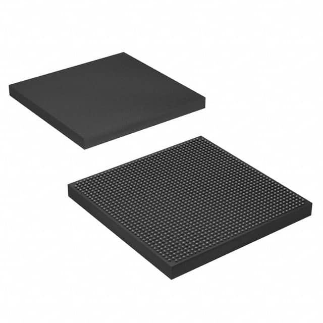
5SGXMB6R2F40I3N
Product Overview
Category
The 5SGXMB6R2F40I3N belongs to the category of Field Programmable Gate Arrays (FPGAs).
Use
This FPGA is commonly used in various electronic applications that require high-performance and flexible digital logic circuits.
Characteristics
- High-performance programmable logic device
- Offers flexibility in designing complex digital systems
- Provides reconfigurability for easy modifications and upgrades
- Supports a wide range of applications
- Offers high-speed data processing capabilities
Package
The 5SGXMB6R2F40I3N comes in a compact package designed to fit on printed circuit boards (PCBs). The package ensures proper protection and efficient heat dissipation.
Essence
The essence of this FPGA lies in its ability to provide a customizable and versatile solution for implementing complex digital designs.
Packaging/Quantity
The 5SGXMB6R2F40I3N is typically packaged individually and is available in various quantities depending on the customer's requirements.
Specifications
- Logic Elements: 220,000
- Embedded Memory: 8,062 Kbits
- Maximum User I/O Pins: 622
- Maximum User I/O Banks: 24
- Clock Networks: 16
- DSP Blocks: 1,288
- Total RAM Bits: 9,437,184 bits
- Operating Voltage: 1.2V
- Operating Temperature Range: -40°C to +100°C
Detailed Pin Configuration
The detailed pin configuration of the 5SGXMB6R2F40I3N can be found in the product datasheet provided by the manufacturer. It includes information about input/output pins, power supply pins, clock pins, and other relevant connections.
Functional Features
- High-speed data processing capabilities
- Configurable logic elements for custom designs
- Embedded memory blocks for efficient data storage
- Dedicated DSP blocks for complex mathematical operations
- Flexible I/O banks for interfacing with external devices
- Clock networks for precise timing control
Advantages and Disadvantages
Advantages
- High performance and flexibility
- Reconfigurable for easy modifications and upgrades
- Wide range of applications
- Efficient use of resources
- Reliable and robust design
Disadvantages
- Steep learning curve for beginners
- Higher cost compared to other programmable logic devices
- Requires specialized tools and software for development
Working Principles
The 5SGXMB6R2F40I3N operates based on the principles of digital logic circuits. It consists of configurable logic elements, embedded memory blocks, DSP blocks, and I/O banks. These components can be interconnected and programmed to implement various digital functions.
The FPGA is configured using a Hardware Description Language (HDL) such as VHDL or Verilog. The HDL code is synthesized and then loaded onto the FPGA, which configures the internal circuitry accordingly. Once programmed, the FPGA performs the desired digital functions based on the input signals received.
Detailed Application Field Plans
The 5SGXMB6R2F40I3N finds applications in various fields, including but not limited to: - Telecommunications - Data processing and networking - Industrial automation - Aerospace and defense - Medical equipment - Automotive electronics
In telecommunications, this FPGA can be used for high-speed data transmission, signal processing, and protocol implementation. In industrial automation, it can be utilized for control systems, monitoring, and data acquisition. In aerospace and defense, it can be employed for radar systems, image processing, and encryption algorithms.
Detailed and Complete Alternative Models
- 5SGXEB6R2F40I3N
- 5SGXAB6R2F40I3N
- 5SGXCB6R2F40I3N
- 5SGXDB6R2F40I3N
These alternative models offer similar functionality and performance characteristics to the 5SGXMB6R2F40I3N. The choice of model depends on specific project requirements and availability.
In conclusion, the 5SGXMB6R2F40I3N is a high-performance FPGA that provides flexibility and reconfigurability for implementing complex digital designs. Its wide range of applications, functional features, and advantages make it a popular choice in various industries.
قم بإدراج 10 أسئلة وإجابات شائعة تتعلق بتطبيق 5SGXMB6R2F40I3N في الحلول التقنية
Sure! Here are 10 common questions and answers related to the application of 5SGXMB6R2F40I3N in technical solutions:
1. What is the 5SGXMB6R2F40I3N FPGA used for? The 5SGXMB6R2F40I3N is a Field-Programmable Gate Array (FPGA) that can be used in various technical solutions, including high-performance computing, networking, telecommunications, and industrial automation.
2. What are the key features of the 5SGXMB6R2F40I3N FPGA? Some key features of this FPGA include a large number of logic elements, high-speed transceivers, embedded memory blocks, DSP blocks, and support for various communication protocols.
3. Can the 5SGXMB6R2F40I3N FPGA be programmed? Yes, the 5SGXMB6R2F40I3N FPGA is programmable. It can be configured using Hardware Description Languages (HDLs) such as VHDL or Verilog.
4. How can the 5SGXMB6R2F40I3N FPGA be integrated into a system? The FPGA can be integrated into a system by connecting it to other components through various interfaces such as PCIe, Ethernet, USB, or custom interfaces using general-purpose I/O pins.
5. What are some typical applications of the 5SGXMB6R2F40I3N FPGA? This FPGA can be used in applications like high-frequency trading, software-defined networking, video processing, signal processing, data center acceleration, and advanced driver-assistance systems (ADAS).
6. Does the 5SGXMB6R2F40I3N FPGA support high-speed data transfer? Yes, the FPGA supports high-speed data transfer through its built-in transceivers, which can operate at multi-gigabit per second rates.
7. Can the 5SGXMB6R2F40I3N FPGA be reprogrammed after deployment? Yes, FPGAs are known for their reprogrammability. The 5SGXMB6R2F40I3N FPGA can be reprogrammed multiple times to adapt to changing requirements or to fix bugs in the design.
8. What development tools are available for programming the 5SGXMB6R2F40I3N FPGA? Intel Quartus Prime is the primary development tool used for programming and configuring the 5SGXMB6R2F40I3N FPGA. It provides a complete suite of design and verification tools.
9. Are there any limitations or considerations when using the 5SGXMB6R2F40I3N FPGA? Some considerations include power consumption, thermal management, and the need for expertise in FPGA design. Additionally, the availability of specific features may vary depending on the specific variant of the FPGA.
10. Where can I find more information about the 5SGXMB6R2F40I3N FPGA? You can find more detailed information about the 5SGXMB6R2F40I3N FPGA, including datasheets, user guides, and application notes, on the official Intel website or by contacting Intel's customer support.


