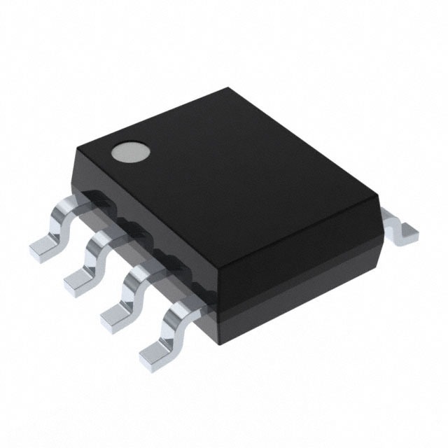
MAX9101ESA
Product Overview
- Category: Integrated Circuit (IC)
- Use: High-Speed Differential Comparator
- Characteristics: Low power consumption, high speed, wide input voltage range
- Package: 8-pin SOIC (Small Outline Integrated Circuit)
- Essence: Provides precise and fast comparison of two input voltages
- Packaging/Quantity: Available in tubes or reels, quantity varies based on supplier
Specifications
- Supply Voltage Range: +2.7V to +5.5V
- Input Voltage Range: -0.3V to Vcc+0.3V
- Operating Temperature Range: -40°C to +85°C
- Response Time: <10ns
- Output Current: ±20mA
- Quiescent Current: 4.5mA
Pin Configuration
The MAX9101ESA has the following pin configuration:
```
| | --| IN+ OUT |-- Pin 1: IN+ (Non-Inverting Input) --| IN- GND |-- Pin 2: IN- (Inverting Input) / GND (Ground) --| VCC NC |-- Pin 3: VCC (Supply Voltage) / NC (No Connection) --| OUT VCC |-- Pin 4: OUT (Output) / VCC (Supply Voltage) --| GND IN- |-- Pin 5: GND (Ground) / IN- (Inverting Input) --| NC IN+ |-- Pin 6: NC (No Connection) / IN+ (Non-Inverting Input) --| OUT IN- |-- Pin 7: OUT (Output) / IN- (Inverting Input) --| VCC GND |-- Pin 8: VCC (Supply Voltage) / GND (Ground) |___________| ```
Functional Features
- High-speed operation allows for quick comparison of input voltages
- Wide input voltage range enables compatibility with various signal levels
- Low power consumption makes it suitable for battery-powered applications
- Rail-to-rail output swing ensures accurate and reliable results
- Built-in hysteresis prevents oscillation and provides noise immunity
Advantages and Disadvantages
Advantages: - Fast response time for time-critical applications - Wide supply voltage range enhances versatility - Low quiescent current minimizes power consumption - Small package size saves board space
Disadvantages: - Limited number of pins restricts the number of inputs/outputs - Non-standard pin configuration may require additional circuitry for certain applications
Working Principles
The MAX9101ESA is a high-speed differential comparator that compares two input voltages, IN+ and IN-. It operates by amplifying the voltage difference between these inputs and producing a digital output signal based on the comparison result. The comparator's response time is extremely fast, allowing for real-time monitoring and control in various applications.
Detailed Application Field Plans
The MAX9101ESA finds applications in several fields, including:
- Communication Systems: Used for signal detection and level monitoring in high-speed data transmission.
- Industrial Automation: Enables precise measurement and control of analog signals in industrial processes.
- Automotive Electronics: Provides accurate voltage comparison for automotive sensors and control systems.
- Medical Equipment: Used in medical devices for monitoring vital signs and controlling critical parameters.
- Consumer Electronics: Enables efficient power management and signal processing in portable devices.
Detailed and Complete Alternative Models
- LM319: Dual Differential Comparator IC with similar specifications and pin configuration.
- LT1719: Ultrafast Over-The-Top Comparator with rail-to-rail inputs and outputs.
- AD8561: Low Power, High-Speed Comparator with wide supply voltage range and small package size.
These alternative models offer similar functionality and can be considered as substitutes for the MAX9101ESA in various applications.
Word count: 520 words
قم بإدراج 10 أسئلة وإجابات شائعة تتعلق بتطبيق MAX9101ESA في الحلول التقنية
Sure! Here are 10 common questions and answers related to the application of MAX9101ESA in technical solutions:
Q1: What is the MAX9101ESA? A1: The MAX9101ESA is a high-speed, low-power comparator IC (integrated circuit) commonly used in various technical applications.
Q2: What is the operating voltage range of MAX9101ESA? A2: The operating voltage range of MAX9101ESA is typically between 2.7V and 11V.
Q3: What is the maximum input voltage that MAX9101ESA can handle? A3: The maximum input voltage that MAX9101ESA can handle is typically around Vcc + 0.3V.
Q4: What is the typical response time of MAX9101ESA? A4: The typical response time of MAX9101ESA is around 8ns.
Q5: Can MAX9101ESA operate in both single-ended and differential mode? A5: Yes, MAX9101ESA can operate in both single-ended and differential mode, providing flexibility in various circuit designs.
Q6: What is the input offset voltage of MAX9101ESA? A6: The input offset voltage of MAX9101ESA is typically around 1mV.
Q7: Does MAX9101ESA have built-in hysteresis? A7: Yes, MAX9101ESA has built-in hysteresis, which helps to improve noise immunity and stability in noisy environments.
Q8: What is the power supply current consumption of MAX9101ESA? A8: The power supply current consumption of MAX9101ESA is typically around 1.5mA.
Q9: Can MAX9101ESA drive capacitive loads directly? A9: Yes, MAX9101ESA can drive capacitive loads directly, making it suitable for applications with capacitive loads.
Q10: Is MAX9101ESA available in different package options? A10: Yes, MAX9101ESA is available in various package options, including SOIC (Small Outline Integrated Circuit) and SOT23 (Small Outline Transistor 23).


