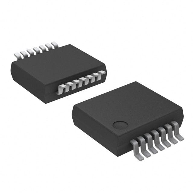
Encyclopedia Entry: 74ABT04DB,118
Product Information Overview
Category: Integrated Circuit (IC)
Use: The 74ABT04DB,118 is a hex inverter IC that is commonly used in digital electronics circuits. It is designed to convert logic level signals, providing an inverted output for each input.
Characteristics: - High-speed operation - Low power consumption - Wide operating voltage range - Schmitt-trigger inputs for noise immunity - Balanced propagation delays - TTL-compatible inputs and outputs
Package: The 74ABT04DB,118 is available in a small outline package (SO) with 14 pins.
Essence: This IC is essential for signal inversion in digital circuits, ensuring proper functioning of various electronic devices.
Packaging/Quantity: The 74ABT04DB,118 is typically sold in reels or tubes containing multiple units. The exact quantity may vary depending on the supplier.
Specifications
- Supply Voltage Range: 4.5V to 5.5V
- Input Voltage Range: 0V to VCC
- Output Voltage Range: 0V to VCC
- Operating Temperature Range: -40°C to +85°C
- Maximum Propagation Delay: 6 ns
- Maximum Quiescent Current: 10 μA
Detailed Pin Configuration
The 74ABT04DB,118 has a total of 14 pins, numbered as follows:
- Input A1
- Output Y1
- Input A2
- Output Y2
- Input A3
- Output Y3
- Ground (GND)
- Output Y4
- Input A4
- Output Y5
- Input A5
- Output Y6
- VCC (Supply Voltage)
- Input A6
Functional Features
- Hex inverter with six independent inverters
- High-speed operation allows for efficient signal processing
- Schmitt-trigger inputs provide noise immunity and improved signal integrity
- Balanced propagation delays ensure synchronized output signals
- TTL-compatible inputs and outputs allow for easy integration with other digital circuits
Advantages and Disadvantages
Advantages: - High-speed operation enables fast data processing - Low power consumption for energy-efficient designs - Wide operating voltage range provides flexibility in various applications - Schmitt-trigger inputs enhance noise immunity, ensuring reliable signal conversion - Balanced propagation delays enable synchronized output signals
Disadvantages: - Limited number of inverters per IC (six in this case) - May require additional components for complex circuit designs
Working Principles
The 74ABT04DB,118 operates based on the principle of signal inversion. Each input signal is inverted, meaning a logic high input will result in a logic low output, and vice versa. This is achieved through the internal circuitry of the hex inverter.
Detailed Application Field Plans
The 74ABT04DB,118 finds application in various digital electronics systems, including but not limited to: - Microcontrollers and microprocessors - Communication devices - Data transmission systems - Signal processing circuits - Logic level conversion circuits
Detailed and Complete Alternative Models
Some alternative models that serve similar functions to the 74ABT04DB,118 include: - 74HC04: A hex inverter IC with similar characteristics but different voltage specifications. - CD4049: A hex inverting buffer IC with enhanced noise immunity and wider voltage range. - SN74LS04: A hex inverter IC compatible with TTL logic levels.
These alternative models can be considered depending on specific project requirements and compatibility with existing circuit designs.
Word Count: 411
قم بإدراج 10 أسئلة وإجابات شائعة تتعلق بتطبيق 74ABT04DB,118 في الحلول التقنية
Sure! Here are 10 common questions and answers related to the application of 74ABT04DB,118 in technical solutions:
Q: What is the 74ABT04DB,118? A: The 74ABT04DB,118 is a hex inverter IC (Integrated Circuit) that consists of six independent inverters.
Q: What is the operating voltage range for the 74ABT04DB,118? A: The operating voltage range for the 74ABT04DB,118 is typically between 4.5V and 5.5V.
Q: What is the maximum output current of the 74ABT04DB,118? A: The maximum output current of the 74ABT04DB,118 is typically around 32mA.
Q: Can the 74ABT04DB,118 be used in both digital and analog circuits? A: No, the 74ABT04DB,118 is specifically designed for digital applications and may not perform optimally in analog circuits.
Q: What is the propagation delay of the 74ABT04DB,118? A: The propagation delay of the 74ABT04DB,118 is typically around 3.5ns.
Q: Can the 74ABT04DB,118 be used as a level shifter? A: Yes, the 74ABT04DB,118 can be used as a level shifter to convert signals from one voltage level to another.
Q: Is the 74ABT04DB,118 compatible with TTL (Transistor-Transistor Logic) inputs? A: Yes, the 74ABT04DB,118 is compatible with TTL inputs and can be used as a drop-in replacement for TTL inverters.
Q: Can the 74ABT04DB,118 drive capacitive loads? A: Yes, the 74ABT04DB,118 can drive small capacitive loads without any additional buffering.
Q: What is the power consumption of the 74ABT04DB,118? A: The power consumption of the 74ABT04DB,118 is typically low, making it suitable for battery-powered applications.
Q: Are there any specific precautions to consider when using the 74ABT04DB,118? A: It is important to ensure that the power supply voltage does not exceed the specified range and to avoid exceeding the maximum ratings for input and output currents to prevent damage to the IC.
Please note that the answers provided here are general and may vary depending on the specific datasheet and manufacturer's specifications for the 74ABT04DB,118.


