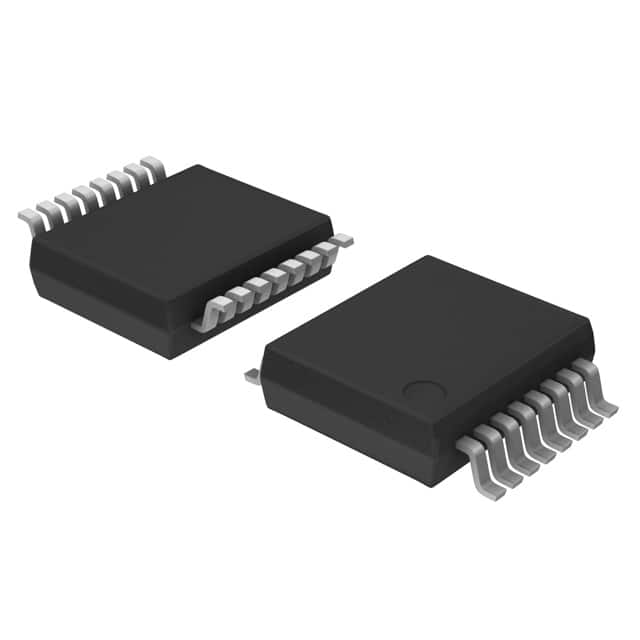
74HC367DB,112
Product Overview
- Category: Integrated Circuit (IC)
- Use: Logic Level Converter
- Characteristics: High-speed operation, low power consumption
- Package: SSOP (Shrink Small Outline Package)
- Essence: Hex Buffer/Line Driver with 3-State Outputs
- Packaging/Quantity: Tape and Reel, 2500 pieces per reel
Specifications
- Supply Voltage Range: 2V to 6V
- Input Voltage Range: 0V to VCC
- Output Voltage Range: 0V to VCC
- Maximum Operating Frequency: 80 MHz
- Number of Inputs: 6
- Number of Outputs: 6
- Output Current: ±6 mA
- Propagation Delay Time: 8 ns
- Operating Temperature Range: -40°C to +125°C
Detailed Pin Configuration
The 74HC367DB,112 has a total of 16 pins. The pin configuration is as follows:
- OE (Output Enable) 1
- A1 (Input) 1
- Y1 (Output) 1
- A2 (Input) 2
- Y2 (Output) 2
- GND (Ground)
- Y3 (Output) 3
- A3 (Input) 3
- Y4 (Output) 4
- A4 (Input) 4
- VCC (Supply Voltage)
- Y5 (Output) 5
- A5 (Input) 5
- Y6 (Output) 6
- A6 (Input) 6
- OE (Output Enable) 2
Functional Features
- Hex buffer with 3-state outputs
- Converts logic levels between different voltage domains
- Enables bidirectional communication between devices operating at different voltage levels
- High-speed operation allows for efficient data transfer
- Low power consumption ensures energy efficiency
Advantages and Disadvantages
Advantages: - Supports a wide supply voltage range, making it versatile for various applications - Provides 3-state outputs, allowing multiple devices to share a common bus - High-speed operation enables fast data transmission - Low power consumption reduces energy usage
Disadvantages: - Limited number of inputs and outputs (6 each) - Propagation delay time may affect timing-sensitive applications
Working Principles
The 74HC367DB,112 is a hex buffer with 3-state outputs. It operates by receiving input signals from one voltage domain and converting them to the corresponding logic levels in another voltage domain. The output enable pins (OE) control the state of the outputs, allowing them to be either active or in a high-impedance state.
When the OE pin is low, the outputs are enabled and reflect the input signals. Conversely, when the OE pin is high, the outputs are disabled and enter a high-impedance state, effectively disconnecting them from the circuit.
Detailed Application Field Plans
The 74HC367DB,112 can be used in various applications, including:
- Level shifting in mixed-voltage systems
- Interfacing between microcontrollers and peripheral devices
- Bus buffering in multiprocessor systems
- Signal isolation in industrial automation
- Logic level conversion in communication interfaces
Detailed and Complete Alternative Models
Some alternative models that serve similar purposes to the 74HC367DB,112 include:
- SN74LVC1T45DBVR - Single-Bit Dual-Supply Bus Transceiver
- CD4050BE - Hex Non-Inverting Buffer/Converter
- TXB0108PWR - 8-Bit Bidirectional Voltage-Level Translator
These alternatives offer similar functionality and can be used as replacements depending on specific requirements.
In conclusion, the 74HC367DB,112 is a versatile logic level converter IC that enables bidirectional communication between devices operating at different voltage levels. With its high-speed operation, low power consumption, and compact SSOP package, it finds applications in various fields such as mixed-voltage systems, microcontroller interfacing, and industrial automation.
قم بإدراج 10 أسئلة وإجابات شائعة تتعلق بتطبيق 74HC367DB,112 في الحلول التقنية
Sure! Here are 10 common questions and answers related to the application of 74HC367DB,112 in technical solutions:
Q: What is the 74HC367DB,112? A: The 74HC367DB,112 is a high-speed hex buffer with 3-state outputs, commonly used in digital logic applications.
Q: What is the maximum operating voltage for the 74HC367DB,112? A: The maximum operating voltage for the 74HC367DB,112 is typically 5.5V.
Q: How many buffers are there in the 74HC367DB,112? A: The 74HC367DB,112 has six buffers, each with an independent 3-state output.
Q: What is the purpose of the 3-state outputs in the 74HC367DB,112? A: The 3-state outputs allow the buffers to be disabled, effectively disconnecting them from the output bus.
Q: What is the maximum output current that the 74HC367DB,112 can drive? A: The 74HC367DB,112 can typically drive up to 25mA of output current per buffer.
Q: Can the 74HC367DB,112 be used in both TTL and CMOS logic systems? A: Yes, the 74HC367DB,112 is compatible with both TTL and CMOS logic levels.
Q: What is the propagation delay of the 74HC367DB,112? A: The propagation delay of the 74HC367DB,112 is typically around 8ns.
Q: Can the 74HC367DB,112 be used as a level shifter? A: Yes, the 74HC367DB,112 can be used as a level shifter to convert signals between different voltage levels.
Q: Is the 74HC367DB,112 suitable for high-speed applications? A: Yes, the 74HC367DB,112 is designed for high-speed operation and can be used in applications with fast switching requirements.
Q: Are there any specific precautions to consider when using the 74HC367DB,112? A: It is important to ensure that the power supply voltage does not exceed the maximum specified value and to avoid exceeding the maximum output current ratings to prevent damage to the device.
Please note that the answers provided here are general and may vary depending on the specific datasheet and manufacturer's specifications for the 74HC367DB,112.


