

74LCX541BQX
Product Overview
- Category: Integrated Circuit (IC)
- Use: Logic Level Shifter
- Characteristics: Low Voltage, High-Speed CMOS Technology
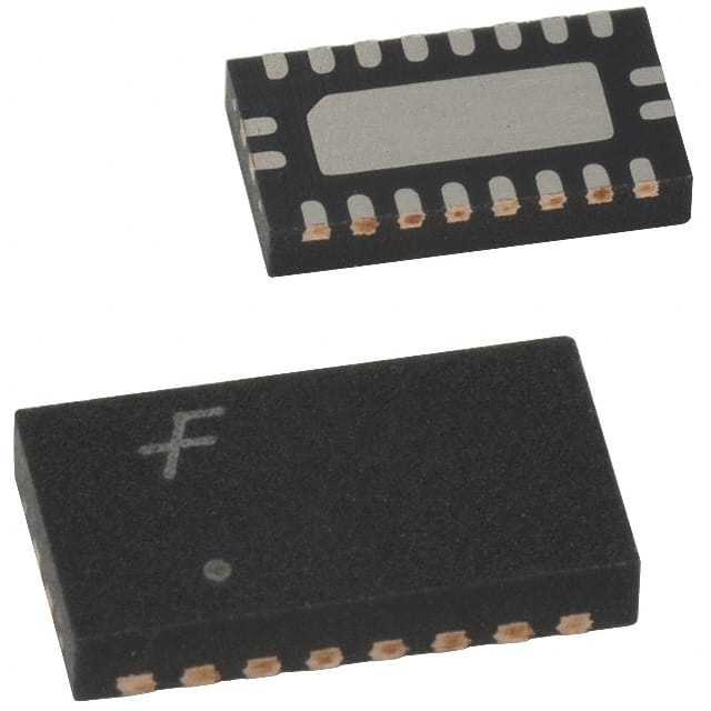
- Package: TSSOP (Thin Shrink Small Outline Package)
- Essence: Bidirectional Octal Buffer/Line Driver with 5V Tolerant Inputs and Outputs
- Packaging/Quantity: Tape and Reel, 2500 units per reel
Specifications
- Supply Voltage Range: 2.3V to 3.6V
- High-Level Input Voltage: 2.0V (Minimum), 3.6V (Maximum)
- Low-Level Input Voltage: -0.3V (Minimum), 0.8V (Maximum)
- High-Level Output Voltage: 2.4V (Minimum), VCC (Maximum)
- Low-Level Output Voltage: 0V (Minimum), 0.4V (Maximum)
- Maximum Input Current: ±10mA
- Maximum Output Current: ±24mA
- Propagation Delay Time: 2.1ns (Typical)
- Operating Temperature Range: -40°C to +85°C
Detailed Pin Configuration
The 74LCX541BQX IC has a total of 20 pins, which are arranged as follows:
┌───┬───┐
   OE ─┤1  └─ 20┬─ VCC
  A1  ─┤2      19├─ GND
  A2  ─┤3      18├─ B1
  A3  ─┤4      17├─ B2
  A4  ─┤5      16├─ B3
  A5  ─┤6      15├─ B4
  A6  ─┤7      14├─ B5
  A7  ─┤8      13├─ B6
  G1  ─┤9      12├─ B7
  G2  ─┤10     11├─ B8
       └───────┘
Functional Features
- Bidirectional buffer/line driver with 3-state outputs
- Inputs and outputs are 5V tolerant, allowing direct interfacing with 5V systems
- Provides non-inverting level shifting between 3.3V and 5V logic levels
- Supports high-speed data transmission with low propagation delay time
- Enables easy expansion of bus lines in digital systems
Advantages and Disadvantages
Advantages: - Wide supply voltage range allows compatibility with various systems - 5V tolerance simplifies interfacing with different logic levels - High-speed CMOS technology ensures fast data transmission - Non-inverting buffer minimizes signal distortion - Compact TSSOP package saves board space
Disadvantages: - Limited output current may restrict use in certain applications - Not suitable for high-voltage environments
Working Principles
The 74LCX541BQX is designed to shift logic levels bidirectionally between 3.3V and 5V systems. It acts as a buffer/line driver, amplifying and transmitting digital signals without inverting their logic states. The IC features 3-state outputs, which can be enabled or disabled using the Output Enable (OE) pin. When disabled, the outputs enter a high-impedance state, allowing multiple devices to share a common bus.
Detailed Application Field Plans
The 74LCX541BQX is commonly used in various digital systems that require level shifting between 3.3V and 5V logic levels. Some typical application fields include:
- Microcontroller interfacing with 5V peripherals
- Communication interfaces (UART, SPI, I2C) between different voltage domains
- Memory address and data bus expansion in embedded systems
- Signal buffering in mixed-voltage systems
- Level translation in battery-powered devices
Detailed and Complete Alternative Models
- SN74LVC541A: Octal Buffer/Line Driver with 3-State Outputs
- MC74LCX541: Low Voltage CMOS Octal Buffer/Line Driver
- CD74HC541: High-Speed CMOS Logic Octal Buffer/Line Driver
- 74HCT541: Octal Buffer/Line Driver with 3-State Outputs
These alternative models offer similar functionality and can be considered as replacements for the 74LCX541BQX in different applications.
Word count: 529 words
قم بإدراج 10 أسئلة وإجابات شائعة تتعلق بتطبيق 74LCX541BQX في الحلول التقنية
Sure! Here are 10 common questions and answers related to the application of 74LCX541BQX in technical solutions:
Question: What is the 74LCX541BQX?
- Answer: The 74LCX541BQX is a high-performance octal buffer/line driver with 3-state outputs.Question: What is the voltage supply range for the 74LCX541BQX?
- Answer: The voltage supply range for this IC is typically between 2.0V and 3.6V.Question: How many inputs and outputs does the 74LCX541BQX have?
- Answer: It has 8 inputs and 8 outputs.Question: Can the 74LCX541BQX be used as a level shifter?
- Answer: Yes, it can be used as a level shifter to convert signals between different voltage levels.Question: What is the maximum output current of the 74LCX541BQX?
- Answer: The maximum output current is typically 24mA.Question: Is the 74LCX541BQX compatible with TTL logic levels?
- Answer: Yes, it is compatible with both TTL and CMOS logic levels.Question: Can I use the 74LCX541BQX in a bidirectional bus application?
- Answer: No, this IC is unidirectional and cannot be used for bidirectional bus applications.Question: What is the propagation delay of the 74LCX541BQX?
- Answer: The typical propagation delay is around 3.5ns.Question: Does the 74LCX541BQX have internal pull-up or pull-down resistors?
- Answer: No, it does not have internal pull-up or pull-down resistors.Question: Can I use the 74LCX541BQX in automotive applications?
- Answer: Yes, this IC is suitable for automotive applications as it meets the necessary standards and requirements.
Please note that these answers are general and may vary depending on the specific datasheet and manufacturer's specifications of the 74LCX541BQX.