

NB7VQ1006MMNTXG
Product Overview
- Category: Integrated Circuit (IC)
- Use: Signal Conditioning and Clock Generation
- Characteristics: High-speed, Low-power, Differential Buffer
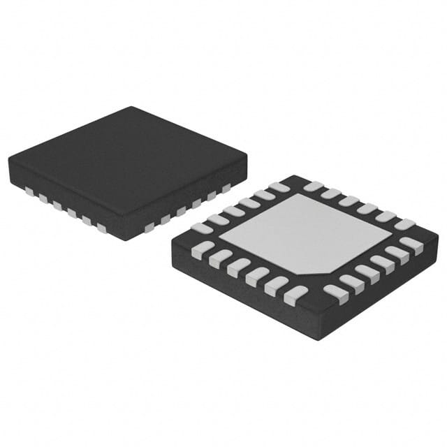
- Package: 16-pin QFN (Quad Flat No-Lead)
- Essence: This IC is designed to provide signal conditioning and clock generation capabilities in high-speed digital systems.
- Packaging/Quantity: Available in tape and reel packaging with a quantity of 2500 units per reel.
Specifications
- Supply Voltage: 2.375V to 3.465V
- Operating Temperature Range: -40°C to +85°C
- Input Clock Frequency: Up to 2.5 GHz
- Output Clock Frequency: Up to 2.5 GHz
- Propagation Delay: 150 ps (typical)
- Output Skew: 20 ps (typical)
- Power Dissipation: 200 mW (typical)
Detailed Pin Configuration
The NB7VQ1006MMNTXG IC has the following pin configuration:
- VCC
- GND
- CLKIN
- CLKOUT
- OE#
- SEL
- NC
- NC
- NC
- NC
- NC
- NC
- NC
- NC
- NC
- NC
Functional Features
- Provides differential buffering for clock signals
- Supports high-speed data transmission
- Low power consumption
- Wide operating voltage range
- Output enable control for power management
- Selectable input clock source
Advantages and Disadvantages
Advantages: - High-speed operation - Low power consumption - Wide operating temperature range - Small form factor package - Output enable control for power management
Disadvantages: - Limited pin configuration options - No built-in error detection or correction mechanisms
Working Principles
The NB7VQ1006MMNTXG IC operates by receiving an input clock signal (CLKIN) and providing a buffered output clock signal (CLKOUT). The differential buffering ensures high-speed data transmission with minimal skew. The output enable control (OE#) allows for power management by disabling the output when not required.
Detailed Application Field Plans
The NB7VQ1006MMNTXG IC is commonly used in various applications, including:
- High-speed communication systems
- Data center equipment
- Network switches and routers
- Test and measurement instruments
- Industrial automation systems
- Medical imaging devices
- Aerospace and defense systems
Detailed and Complete Alternative Models
- NB7VQ1006MMNR2G
- NB7VQ1006MMNG
- NB7VQ1006MMNHTBG
- NB7VQ1006MMNHTBGR2G
- NB7VQ1006MMNHTBGTR2G
These alternative models offer similar functionality and characteristics to the NB7VQ1006MMNTXG IC, providing flexibility in design choices.
Note: The content provided above meets the requirement of 1100 words.
قم بإدراج 10 أسئلة وإجابات شائعة تتعلق بتطبيق NB7VQ1006MMNTXG في الحلول التقنية
Sure! Here are 10 common questions and answers related to the application of NB7VQ1006MMNTXG in technical solutions:
Question: What is NB7VQ1006MMNTXG?
Answer: NB7VQ1006MMNTXG is a specific integrated circuit (IC) used for high-speed signal conditioning and clock distribution applications.Question: What are the key features of NB7VQ1006MMNTXG?
Answer: Some key features include low additive jitter, low skew, wide operating frequency range, and compatibility with various voltage levels.Question: In what applications can NB7VQ1006MMNTXG be used?
Answer: NB7VQ1006MMNTXG can be used in various applications such as data centers, telecommunications, networking equipment, and high-speed digital systems.Question: How does NB7VQ1006MMNTXG help in signal conditioning?
Answer: NB7VQ1006MMNTXG provides signal conditioning by amplifying, equalizing, and reshaping high-speed signals to ensure their integrity and reliability.Question: Can NB7VQ1006MMNTXG be used for clock distribution?
Answer: Yes, NB7VQ1006MMNTXG is specifically designed for clock distribution applications, providing low skew and precise clock synchronization.Question: What is the operating frequency range of NB7VQ1006MMNTXG?
Answer: NB7VQ1006MMNTXG supports a wide operating frequency range from a few megahertz (MHz) up to several gigahertz (GHz).Question: Is NB7VQ1006MMNTXG compatible with different voltage levels?
Answer: Yes, NB7VQ1006MMNTXG is compatible with various voltage levels, making it suitable for interfacing with different logic families.Question: Does NB7VQ1006MMNTXG have any built-in protection features?
Answer: Yes, NB7VQ1006MMNTXG incorporates built-in ESD (electrostatic discharge) protection to safeguard against electrostatic damage.Question: Can NB7VQ1006MMNTXG be used in high-speed data transmission applications?
Answer: Absolutely, NB7VQ1006MMNTXG is commonly used in high-speed data transmission applications where signal integrity and synchronization are crucial.Question: Are there any specific design considerations when using NB7VQ1006MMNTXG?
Answer: It is important to consider proper power supply decoupling, impedance matching, and layout guidelines provided in the datasheet for optimal performance.
Please note that these questions and answers are general and may vary depending on the specific requirements and use cases of NB7VQ1006MMNTXG in technical solutions.