

NC7SV08L6X
Product Overview
- Category: Integrated Circuit (IC)
- Use: Logic Gate
- Characteristics: Low Voltage, High-Speed, Single Gate
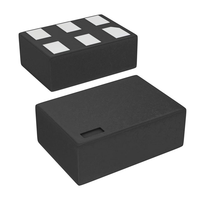
- Package: SOT-23-6
- Essence: AND Gate
- Packaging/Quantity: Tape and Reel, 3000 units per reel
Specifications
- Logic Family: CMOS
- Supply Voltage: 1.65V to 5.5V
- Input Voltage Levels: VIL = 0.3V, VIH = 0.7V
- Output Voltage Levels: VOL = 0.05V, VOH = 4.95V
- Propagation Delay: 2.5ns (typical)
- Operating Temperature Range: -40°C to +85°C
Detailed Pin Configuration
The NC7SV08L6X has a total of 6 pins arranged as follows:
```
| | --|____|-- | | --|____|-- ```
Pin Configuration: 1. Input A 2. Input B 3. GND (Ground) 4. Output Y 5. VCC (Power Supply) 6. Input C
Functional Features
- Performs logical AND operation on three inputs (A, B, and C)
- Provides a single output (Y) based on the input combination
- Supports low voltage operation, making it suitable for battery-powered devices
- Offers high-speed performance, enabling quick signal processing
- Compact SOT-23-6 package allows for space-efficient integration into circuits
Advantages and Disadvantages
Advantages: - Low power consumption due to CMOS technology - Wide supply voltage range enhances versatility - Small form factor enables integration in compact designs - Fast propagation delay ensures efficient signal processing
Disadvantages: - Limited to three inputs, may not be suitable for complex logic operations - Sensitivity to electrostatic discharge (ESD) requires proper handling precautions
Working Principles
The NC7SV08L6X is an AND gate that performs logical conjunction on its three input signals (A, B, and C). It utilizes CMOS technology, which allows for low power consumption and compatibility with a wide range of supply voltages. The gate's internal circuitry processes the input signals and generates a single output (Y) based on the logical AND operation.
Detailed Application Field Plans
The NC7SV08L6X finds applications in various fields where logical AND operations are required. Some potential application areas include:
- Digital Electronics: Used in digital circuits for combining multiple input signals and generating an output based on their logical combination.
- Microcontrollers: Integrated into microcontroller-based systems to perform conditional operations and control external devices based on input conditions.
- Communication Systems: Employed in communication systems for signal processing and decision-making based on multiple input conditions.
- Industrial Automation: Utilized in industrial automation systems for logical control and decision-making based on sensor inputs.
Detailed and Complete Alternative Models
- SN74LVC1G08: Single 2-Input AND Gate, SOT-23 package, operates at 1.65V to 5.5V.
- MC74VHC1G08: Single 2-Input AND Gate, SOT-23 package, operates at 2.0V to 5.5V.
- CD4081B: Quad 2-Input AND Gate, DIP-14 package, operates at 3.0V to 18V.
These alternative models offer similar functionality to the NC7SV08L6X and can be considered as replacements based on specific requirements.
Word count: 346 words
قم بإدراج 10 أسئلة وإجابات شائعة تتعلق بتطبيق NC7SV08L6X في الحلول التقنية
Sure! Here are 10 common questions and answers related to the application of NC7SV08L6X in technical solutions:
Question: What is the NC7SV08L6X?
Answer: The NC7SV08L6X is a single-gate, dual-supply voltage CMOS logic gate.Question: What is the operating voltage range for the NC7SV08L6X?
Answer: The NC7SV08L6X operates within a voltage range of 1.65V to 5.5V.Question: What is the maximum output current of the NC7SV08L6X?
Answer: The NC7SV08L6X has a maximum output current of 32mA.Question: Can the NC7SV08L6X be used in battery-powered applications?
Answer: Yes, the NC7SV08L6X can be used in battery-powered applications due to its low power consumption.Question: What is the propagation delay of the NC7SV08L6X?
Answer: The propagation delay of the NC7SV08L6X is typically around 3.5ns.Question: Can the NC7SV08L6X be used as a level shifter?
Answer: Yes, the NC7SV08L6X can be used as a level shifter to interface between different voltage domains.Question: Is the NC7SV08L6X compatible with other CMOS logic families?
Answer: Yes, the NC7SV08L6X is compatible with other CMOS logic families, making it versatile for various applications.Question: Does the NC7SV08L6X have built-in ESD protection?
Answer: Yes, the NC7SV08L6X has built-in ESD protection, ensuring robustness against electrostatic discharge.Question: Can the NC7SV08L6X be used in high-speed applications?
Answer: Yes, the NC7SV08L6X can be used in high-speed applications due to its fast switching speed.Question: What is the package type of the NC7SV08L6X?
Answer: The NC7SV08L6X is available in a small SOT-23 package, making it suitable for space-constrained designs.
Please note that these answers are general and may vary depending on the specific application and requirements.