

NL17VHC1G07DTT1G
Basic Information Overview
- Category: Integrated Circuit (IC)
- Use: Logic Gate
- Characteristics: High-speed, Low-power consumption
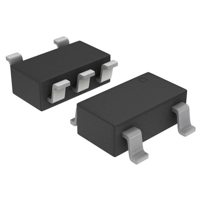
- Package: SOT-353
- Essence: Single Buffer/Driver
- Packaging/Quantity: Tape and Reel, 3000 pieces per reel
Specifications
- Supply Voltage Range: 2.0V to 5.5V
- Input Voltage Range: 0V to VCC
- Output Voltage Range: 0V to VCC
- Operating Temperature Range: -40°C to +125°C
- Propagation Delay Time: 3.8ns (typical)
- Maximum Quiescent Current: 1μA
Detailed Pin Configuration
The NL17VHC1G07DTT1G has the following pin configuration:
____
   A -|    |- VCC
   B -|    |- Y
 GND -|____|- /Y
Functional Features
- Single buffer/driver with open-drain output
- Compatible with TTL and CMOS logic levels
- High-speed operation with low propagation delay
- Low power consumption
- Wide supply voltage range for versatile applications
- ESD protection on all pins
Advantages and Disadvantages
Advantages: - High-speed operation allows for efficient data transmission - Low power consumption extends battery life in portable devices - Versatile supply voltage range enables compatibility with various systems - ESD protection ensures robustness against electrostatic discharge
Disadvantages: - Open-drain output requires external pull-up resistor for proper signal level translation - Limited number of input/output pins restricts complex circuit designs
Working Principles
The NL17VHC1G07DTT1G is a single buffer/driver IC that provides a logic level translation function. It takes an input signal and amplifies it to drive an open-drain output. The open-drain configuration allows for easy interfacing with other devices by connecting the output to a pull-up resistor. When the input is low, the output is pulled low, and when the input is high, the output is in a high-impedance state.
Detailed Application Field Plans
The NL17VHC1G07DTT1G can be used in various applications, including:
- Communication Systems: Signal level translation between different voltage domains in data communication interfaces.
- Industrial Control: Interface between microcontrollers and peripheral devices, such as sensors and actuators.
- Automotive Electronics: Logic level conversion for automotive control units and communication buses.
- Consumer Electronics: Voltage level shifting in audio/video equipment, gaming consoles, and home automation systems.
- Medical Devices: Signal conditioning and level translation in medical monitoring and diagnostic equipment.
Detailed and Complete Alternative Models
- SN74LVC1G07DBVR - Single Buffer/Driver IC from Texas Instruments
- MC74VHC1GT07DF1G - Single Buffer/Driver IC from ON Semiconductor
- 74LVC1G07GW - Single Buffer/Driver IC from NXP Semiconductors
- TC7SZ07FU - Single Buffer/Driver IC from Toshiba Semiconductor
These alternative models offer similar functionality and can be considered as replacements for the NL17VHC1G07DTT1G in various applications.
Word count: 400 words
قم بإدراج 10 أسئلة وإجابات شائعة تتعلق بتطبيق NL17VHC1G07DTT1G في الحلول التقنية
Sure! Here are 10 common questions and answers related to the application of NL17VHC1G07DTT1G in technical solutions:
Q1: What is NL17VHC1G07DTT1G? A1: NL17VHC1G07DTT1G is a specific type of logic gate, specifically an open-drain buffer, which can be used in various technical solutions.
Q2: What is the purpose of NL17VHC1G07DTT1G? A2: The purpose of NL17VHC1G07DTT1G is to provide voltage level shifting and buffering capabilities in digital circuits.
Q3: What voltage levels does NL17VHC1G07DTT1G support? A3: NL17VHC1G07DTT1G supports voltage levels ranging from 1.65V to 5.5V.
Q4: How many inputs and outputs does NL17VHC1G07DTT1G have? A4: NL17VHC1G07DTT1G has one input and one output.
Q5: Can NL17VHC1G07DTT1G be used for bidirectional communication? A5: No, NL17VHC1G07DTT1G is unidirectional and can only be used for one-way data transmission.
Q6: What is the maximum frequency at which NL17VHC1G07DTT1G can operate? A6: NL17VHC1G07DTT1G can operate at a maximum frequency of 200 MHz.
Q7: Is NL17VHC1G07DTT1G compatible with other logic families? A7: Yes, NL17VHC1G07DTT1G is compatible with a wide range of logic families, including CMOS, TTL, and LVCMOS.
Q8: Can NL17VHC1G07DTT1G be used in battery-powered applications? A8: Yes, NL17VHC1G07DTT1G is suitable for battery-powered applications as it has low power consumption.
Q9: What are the typical applications of NL17VHC1G07DTT1G? A9: NL17VHC1G07DTT1G is commonly used in level shifting, voltage translation, and interfacing between different logic levels.
Q10: Is NL17VHC1G07DTT1G available in different package options? A10: Yes, NL17VHC1G07DTT1G is available in various package options, such as SOT-23 and SC-70, to suit different design requirements.
Please note that these answers are general and may vary depending on specific technical requirements and datasheet specifications.