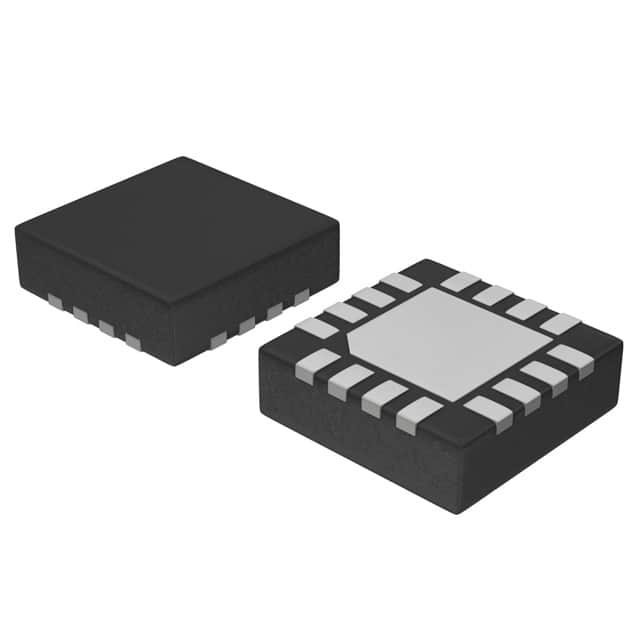
NLAS9099MN1R2G
Basic Information Overview
- Category: Integrated Circuit (IC)
- Use: Analog Switch
- Characteristics: Low voltage, high-speed, dual SPDT switch
- Package: Miniature 8-pin package (DFN)
- Essence: Provides a compact and efficient solution for signal routing applications
- Packaging/Quantity: Available in tape and reel packaging, quantity varies based on customer requirements
Specifications
- Supply Voltage Range: 1.65V to 5.5V
- On-Resistance: 0.6Ω (typical) at 3.3V supply voltage
- Bandwidth: 400MHz (-3dB)
- Crosstalk Rejection: -60dB at 1MHz
- Leakage Current: 1nA (typical) at 3.3V supply voltage
- Operating Temperature Range: -40°C to +85°C
Detailed Pin Configuration
The NLAS9099MN1R2G has the following pin configuration:
```
| | --| IN1 OUT1 |-- Pin 1: Input 1 / Output 1 --| IN2 OUT2 |-- Pin 2: Input 2 / Output 2 --| VDD GND |-- Pin 3: Power Supply (+) / Ground (-) --| IN4 OUT4 |-- Pin 4: Input 4 / Output 4 --| IN3 OUT3 |-- Pin 5: Input 3 / Output 3 --| NC NC |-- Pin 6: No Connection --| EN NC |-- Pin 7: Enable Control / No Connection --| NC VDD |-- Pin 8: No Connection / Power Supply (+) |___________| ```
Functional Features
- Dual SPDT switch with low on-resistance and high bandwidth
- Wide supply voltage range allows compatibility with various systems
- Low leakage current ensures minimal power consumption
- High crosstalk rejection for improved signal integrity
- Enable control pin for easy switching between ON/OFF states
Advantages and Disadvantages
Advantages: - Compact and miniature package for space-constrained applications - Low voltage operation suitable for battery-powered devices - High-speed switching capability for time-critical applications - Excellent signal quality with low crosstalk and leakage current
Disadvantages: - Limited number of channels (4 inputs/outputs) - Not suitable for high-power applications due to low on-resistance
Working Principles
The NLAS9099MN1R2G is based on CMOS technology, utilizing MOSFET transistors as the switching elements. When the enable control pin (EN) is activated, the internal switches connect the corresponding input pins (IN1-IN4) to their respective output pins (OUT1-OUT4). This allows the signal to pass through the switch, enabling signal routing or multiplexing.
Detailed Application Field Plans
The NLAS9099MN1R2G finds applications in various fields, including but not limited to: 1. Portable electronic devices: Enables signal routing in smartphones, tablets, and wearable devices. 2. Audio/video equipment: Facilitates audio and video signal switching in amplifiers, mixers, and home theater systems. 3. Test and measurement instruments: Provides signal routing capabilities in oscilloscopes, function generators, and data acquisition systems. 4. Industrial automation: Used for signal switching in control panels, PLCs, and industrial sensors. 5. Automotive electronics: Enables signal routing in infotainment systems, navigation units, and vehicle diagnostics.
Detailed and Complete Alternative Models
- NLAS9099MN1R2G is part of the NLAS9099 series, which includes other variants with different package options and pin configurations.
- Alternative models from different manufacturers include ADG1419, MAX4619, and CD4053B.
Note: The above information provides a comprehensive overview of NLAS9099MN1R2G, covering its basic details, specifications, features, applications, and alternative models.
قم بإدراج 10 أسئلة وإجابات شائعة تتعلق بتطبيق NLAS9099MN1R2G في الحلول التقنية
Sure! Here are 10 common questions and answers related to the application of NLAS9099MN1R2G in technical solutions:
Q1: What is NLAS9099MN1R2G? A1: NLAS9099MN1R2G is a specific model number for a high-performance analog switch IC used in various technical solutions.
Q2: What are the key features of NLAS9099MN1R2G? A2: Some key features of NLAS9099MN1R2G include low on-resistance, wide voltage range, low power consumption, and compatibility with different signal types.
Q3: In what applications can NLAS9099MN1R2G be used? A3: NLAS9099MN1R2G can be used in applications such as audio/video signal routing, data acquisition systems, test equipment, medical devices, and industrial automation.
Q4: How does NLAS9099MN1R2G help in audio/video signal routing? A4: NLAS9099MN1R2G allows seamless switching between different audio/video sources, enabling efficient signal routing and management.
Q5: Can NLAS9099MN1R2G handle both analog and digital signals? A5: Yes, NLAS9099MN1R2G is designed to handle both analog and digital signals, making it versatile for various technical solutions.
Q6: What is the voltage range supported by NLAS9099MN1R2G? A6: NLAS9099MN1R2G supports a wide voltage range, typically from -5V to +5V, allowing compatibility with different voltage levels.
Q7: Does NLAS9099MN1R2G consume low power? A7: Yes, NLAS9099MN1R2G is designed to consume low power, making it suitable for battery-powered devices and energy-efficient solutions.
Q8: Can NLAS9099MN1R2G be used in medical devices? A8: Yes, NLAS9099MN1R2G can be used in medical devices where precise signal routing and compatibility with different signal types are required.
Q9: Is NLAS9099MN1R2G suitable for industrial automation applications? A9: Absolutely, NLAS9099MN1R2G's robust design, wide voltage range, and low power consumption make it well-suited for industrial automation systems.
Q10: Are there any specific design considerations when using NLAS9099MN1R2G? A10: It is important to consider factors such as signal integrity, voltage levels, and power supply requirements while designing with NLAS9099MN1R2G to ensure optimal performance in technical solutions.
Please note that the answers provided here are general and may vary based on specific use cases and requirements.


