

NLVU1GT125AMUTCG
Product Overview
- Category: Integrated Circuit
- Use: Logic Gate
- Characteristics: Single Gate, Non-Inverting Buffer
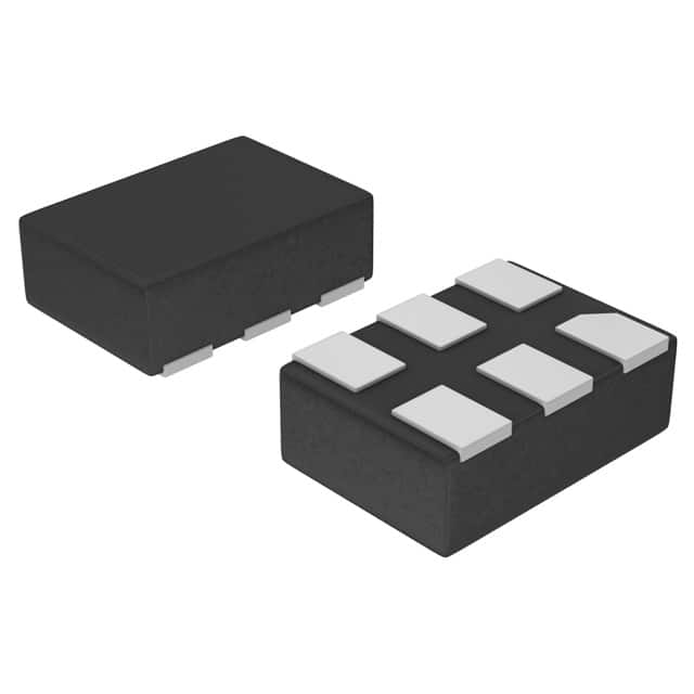
- Package: SOT-23-5
- Essence: High-Speed CMOS Technology
- Packaging/Quantity: Tape and Reel, 3000 units per reel
Specifications
- Supply Voltage: 1.65V to 5.5V
- Input Voltage: 0V to VCC
- Output Voltage: 0V to VCC
- Operating Temperature Range: -40°C to +85°C
- Propagation Delay: 3.4ns (typical)
- Output Drive Capability: ±24mA at 3.3V
Detailed Pin Configuration
The NLVU1GT125AMUTCG has a total of 5 pins arranged as follows:
____
   VCC |    |
   A   |    |
   Y   |    |
   GND |____|
- VCC: Power supply pin (+)
- A: Input pin
- Y: Output pin
- GND: Ground pin (-)
Functional Features
- Non-inverting buffer with high-speed operation
- Wide operating voltage range for compatibility with various systems
- Low power consumption
- High output drive capability for driving capacitive loads
- Schmitt-trigger input for improved noise immunity
Advantages and Disadvantages
Advantages
- High-speed operation allows for efficient signal processing.
- Wide operating voltage range enables compatibility with different power supply levels.
- Low power consumption helps in reducing energy usage.
- High output drive capability ensures reliable performance even with capacitive loads.
- Schmitt-trigger input enhances noise immunity, resulting in more accurate signal processing.
Disadvantages
- Limited number of gates in a single package.
- Sensitive to electrostatic discharge (ESD), requiring proper handling during assembly and usage.
Working Principles
The NLVU1GT125AMUTCG is a non-inverting buffer that amplifies and reshapes digital signals. It operates using high-speed CMOS technology, which allows for fast switching between logic levels. The input signal is buffered and inverted, producing an output signal with the same logic level as the input but with improved drive capability. The Schmitt-trigger input ensures reliable operation even in the presence of noise or signal degradation.
Detailed Application Field Plans
The NLVU1GT125AMUTCG can be used in various applications, including:
- Digital communication systems
- Microcontrollers and microprocessors
- Data transmission and reception circuits
- Signal conditioning and level shifting circuits
- Industrial automation and control systems
- Consumer electronics devices
Detailed and Complete Alternative Models
Some alternative models that offer similar functionality to the NLVU1GT125AMUTCG are:
- SN74LVC1G125DBVR - Texas Instruments
- MC74LCX125DTG - ON Semiconductor
- 74LVC1G125GW - NXP Semiconductors
- TC7SZ125FU - Toshiba Semiconductor
- NC7SZ125P5X - Fairchild Semiconductor
These alternatives provide comparable features and performance, allowing users to choose the most suitable option for their specific requirements.
Word count: 420 words
قم بإدراج 10 أسئلة وإجابات شائعة تتعلق بتطبيق NLVU1GT125AMUTCG في الحلول التقنية
Sure! Here are 10 common questions and answers related to the application of NLVU1GT125AMUTCG in technical solutions:
Q1: What is NLVU1GT125AMUTCG? A1: NLVU1GT125AMUTCG is a specific model of integrated circuit (IC) used for voltage level translation in technical solutions.
Q2: What is the purpose of NLVU1GT125AMUTCG? A2: The purpose of NLVU1GT125AMUTCG is to enable communication between devices operating at different voltage levels by translating signals from one voltage level to another.
Q3: What voltage levels can NLVU1GT125AMUTCG translate between? A3: NLVU1GT125AMUTCG can translate between voltage levels of 1.8V and 5V.
Q4: How does NLVU1GT125AMUTCG achieve voltage level translation? A4: NLVU1GT125AMUTCG uses a combination of MOSFETs and other circuitry to convert signals from one voltage level to another.
Q5: What are some typical applications of NLVU1GT125AMUTCG? A5: NLVU1GT125AMUTCG is commonly used in various technical solutions, such as interfacing between microcontrollers and sensors, communication between different logic families, and level shifting in mixed-voltage systems.
Q6: Can NLVU1GT125AMUTCG handle bidirectional voltage level translation? A6: No, NLVU1GT125AMUTCG is unidirectional and can only translate signals from a lower voltage level to a higher voltage level or vice versa.
Q7: What is the maximum data rate supported by NLVU1GT125AMUTCG? A7: NLVU1GT125AMUTCG can support data rates up to 100 Mbps.
Q8: Is NLVU1GT125AMUTCG compatible with both CMOS and TTL logic levels? A8: Yes, NLVU1GT125AMUTCG is compatible with both CMOS (Complementary Metal-Oxide-Semiconductor) and TTL (Transistor-Transistor Logic) logic levels.
Q9: Does NLVU1GT125AMUTCG require external components for operation? A9: No, NLVU1GT125AMUTCG is a standalone IC and does not require any external components for its basic operation.
Q10: What is the package type of NLVU1GT125AMUTCG? A10: NLVU1GT125AMUTCG is available in a small form factor package, such as SOT-23 or similar, which makes it suitable for space-constrained applications.
Please note that the specific details mentioned above may vary depending on the manufacturer's specifications and datasheet of NLVU1GT125AMUTCG.