

M29F080D90N1
Product Overview
Category
M29F080D90N1 belongs to the category of non-volatile memory devices.
Use
This product is primarily used for data storage in various electronic devices such as computers, smartphones, and embedded systems.
Characteristics
- Non-volatile: The M29F080D90N1 retains stored data even when power is removed.
- High capacity: This device offers a storage capacity of 8 megabits (1 megabyte).
- Fast access time: It provides quick read and write operations, ensuring efficient data transfer.
- Low power consumption: The M29F080D90N1 is designed to consume minimal power during operation.
- Durable: With its robust construction, this memory device can withstand harsh environmental conditions.
Package
The M29F080D90N1 is available in a compact and industry-standard package, making it compatible with various circuit board designs.
Essence
The essence of M29F080D90N1 lies in its ability to reliably store and retrieve digital information, ensuring data integrity and system performance.
Packaging/Quantity
This product is typically packaged in reels or trays, with each containing a specific quantity of M29F080D90N1 devices. The exact quantity may vary depending on the manufacturer's specifications.
Specifications
- Storage Capacity: 8 Megabits (1 Megabyte)
- Supply Voltage: 2.7V - 3.6V
- Access Time:
- Read: 90 ns
- Program: 10 μs
- Erase: 10 ms
- Operating Temperature Range: -40°C to +85°C
- Interface: Parallel
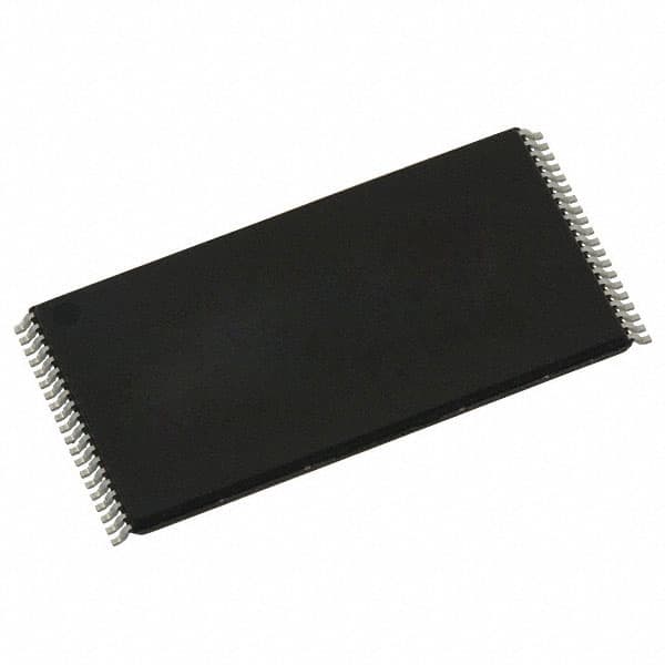
- Package Type: TSOP (Thin Small Outline Package)
Detailed Pin Configuration
The M29F080D90N1 features a parallel interface with the following pin configuration:
- VCC: Power Supply
- A0-A18: Address Inputs
- DQ0-DQ7: Data Input/Output
- WE#: Write Enable
- CE#: Chip Enable
- OE#: Output Enable
- RP#/BYTE#: Reset/Byte Mode Select
- VSS: Ground
Functional Features
- Read Operation: The M29F080D90N1 allows for fast and reliable reading of stored data.
- Program Operation: This device supports programming, enabling users to write new data into the memory.
- Erase Operation: The M29F080D90N1 can be erased, allowing for the removal of previously stored data.
- Protection Mechanism: It includes a protection mechanism to prevent accidental modification or erasure of data.
Advantages and Disadvantages
Advantages
- High storage capacity
- Fast access time
- Low power consumption
- Durable construction
- Reliable data retention
Disadvantages
- Limited write endurance
- Relatively slower erase operation compared to newer memory technologies
Working Principles
The M29F080D90N1 utilizes flash memory technology, which stores data by trapping electric charges within floating gate transistors. These charges represent binary information (0s and 1s) and can be read, programmed, or erased using specific electrical signals.
Detailed Application Field Plans
The M29F080D90N1 finds applications in various fields, including: - Consumer electronics - Automotive systems - Industrial automation - Medical devices - Communication equipment
Detailed and Complete Alternative Models
Some alternative models that offer similar functionality to the M29F080D90N1 include: - M29F080D70N1 - M29F080D120N1 - M29F080D150N1
These models may differ in terms of storage capacity, access time, or package type, providing options to suit specific requirements.
Word count: 520 words
قم بإدراج 10 أسئلة وإجابات شائعة تتعلق بتطبيق M29F080D90N1 في الحلول التقنية
Sure! Here are 10 common questions and answers related to the application of M29F080D90N1 in technical solutions:
Q1: What is M29F080D90N1? A1: M29F080D90N1 is a specific model of flash memory chip commonly used in technical solutions.
Q2: What is the storage capacity of M29F080D90N1? A2: The M29F080D90N1 has a storage capacity of 8 megabits (1 megabyte).
Q3: What is the operating voltage range for M29F080D90N1? A3: The operating voltage range for M29F080D90N1 is typically between 2.7V and 3.6V.
Q4: What is the maximum clock frequency supported by M29F080D90N1? A4: The maximum clock frequency supported by M29F080D90N1 is 90 MHz.
Q5: Can M29F080D90N1 be used for code storage in microcontrollers? A5: Yes, M29F080D90N1 can be used for code storage in microcontrollers as it provides non-volatile memory.
Q6: Is M29F080D90N1 compatible with SPI interface? A6: Yes, M29F080D90N1 supports the Serial Peripheral Interface (SPI) for communication with other devices.
Q7: Does M29F080D90N1 have built-in error correction capabilities? A7: No, M29F080D90N1 does not have built-in error correction capabilities. External error correction techniques may be required.
Q8: Can M29F080D90N1 be used in automotive applications? A8: Yes, M29F080D90N1 is suitable for automotive applications as it can withstand a wide temperature range and has high reliability.
Q9: What is the typical access time of M29F080D90N1? A9: The typical access time of M29F080D90N1 is around 90 nanoseconds.
Q10: Is M29F080D90N1 available in surface mount packages? A10: Yes, M29F080D90N1 is available in various surface mount packages such as TSOP, SOIC, and TFBGA.
Please note that these answers are general and may vary depending on the specific datasheet and manufacturer's specifications for M29F080D90N1.