Encyclopedia Entry: 74AC11008DR
Product Overview
Category
The 74AC11008DR belongs to the category of integrated circuits (ICs), specifically digital logic gates.
Use
This product is commonly used in electronic devices and systems for performing logical operations, such as AND, OR, and NAND.
Characteristics
- The 74AC11008DR is a quad 2-input AND gate.
- It operates on a supply voltage range of 2V to 6V.
- It has a high-speed operation with a propagation delay of 5.5 ns.
- This IC offers low power consumption and high noise immunity.
- It is compatible with both TTL and CMOS logic levels.
Package
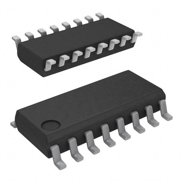
The 74AC11008DR is available in a standard SOIC (Small Outline Integrated Circuit) package.
Essence
The essence of the 74AC11008DR lies in its ability to perform logical AND operations on two input signals, providing an output signal based on their combination.
Packaging/Quantity
This product is typically sold in reels or tubes containing multiple units. The exact quantity may vary depending on the supplier.
Specifications
- Supply Voltage Range: 2V to 6V
- Input Voltage High Level (VIH): 2V to VCC + 0.5V
- Input Voltage Low Level (VIL): -0.5V to 0.8V
- Output Voltage High Level (VOH): VCC - 0.5V
- Output Voltage Low Level (VOL): 0.4V
- Propagation Delay: 5.5 ns (typical)
- Operating Temperature Range: -40°C to 85°C
Detailed Pin Configuration
The 74AC11008DR has a total of 14 pins, which are assigned specific functions as follows:
- Pin 1: Input A1
- Pin 2: Input B1
- Pin 3: Output Y1
- Pin 4: Ground (GND)
- Pin 5: Input A2
- Pin 6: Input B2
- Pin 7: Output Y2
- Pin 8: VCC (Supply Voltage)
- Pin 9: Output Y3
- Pin 10: Input B3
- Pin 11: Input A3
- Pin 12: Output Y4
- Pin 13: Input B4
- Pin 14: Input A4
Functional Features
- The 74AC11008DR performs logical AND operations on the input signals A and B.
- It provides four independent AND gates in a single package.
- Each gate has two inputs and one output.
- The outputs are active-high, meaning they produce a high logic level when the inputs satisfy the AND condition.
Advantages and Disadvantages
Advantages
- High-speed operation enables efficient processing of logical operations.
- Low power consumption helps conserve energy in electronic systems.
- Compatibility with both TTL and CMOS logic levels allows for versatile integration into different circuit designs.
- High noise immunity ensures reliable performance even in noisy environments.
Disadvantages
- Limited to performing only AND operations, which may restrict its applicability in certain scenarios.
- Requires careful consideration of voltage levels to prevent damage or incorrect operation.
Working Principles
The 74AC11008DR operates based on the principles of digital logic. When the input signals A and B are applied to the respective AND gates, the internal circuitry compares their logic levels. If both inputs are at a high logic level, the output will also be high. Otherwise, the output remains low. This behavior follows the logical AND operation.
Detailed Application Field Plans
The 74AC11008DR finds applications in various electronic systems and devices, including but not limited to: - Microprocessors and microcontrollers - Data communication systems - Industrial automation equipment - Consumer electronics - Automotive electronics
Detailed and Complete Alternative Models
Some alternative models that offer similar functionality to the 74AC11008DR include: - 74HC08: Quad 2-input AND gate with CMOS logic levels. - SN74LS08: Quad 2-input AND gate with TTL logic levels. - CD4081: Quad 2-input AND gate with higher voltage tolerance.
These alternatives can be considered based on specific requirements, such as voltage compatibility, speed, or package type.
Word count: 550 words
قم بإدراج 10 أسئلة وإجابات شائعة تتعلق بتطبيق 74AC11008DR في الحلول التقنية
Sure! Here are 10 common questions and answers related to the application of 74AC11008DR in technical solutions:
Q: What is the 74AC11008DR? A: The 74AC11008DR is a quad 2-input AND gate integrated circuit (IC) that can be used in various digital logic applications.
Q: What is the operating voltage range for the 74AC11008DR? A: The operating voltage range for the 74AC11008DR is typically between 2V and 6V.
Q: What is the maximum output current of the 74AC11008DR? A: The maximum output current of the 74AC11008DR is around 24mA.
Q: Can the 74AC11008DR be used in high-speed applications? A: Yes, the 74AC11008DR is designed for high-speed operation and can be used in applications where fast switching times are required.
Q: How many AND gates are there in the 74AC11008DR? A: The 74AC11008DR contains four independent AND gates.
Q: What is the propagation delay of the 74AC11008DR? A: The propagation delay of the 74AC11008DR is typically around 5ns.
Q: Can the 74AC11008DR be used in both CMOS and TTL logic systems? A: Yes, the 74AC11008DR is compatible with both CMOS and TTL logic levels.
Q: What is the power dissipation of the 74AC11008DR? A: The power dissipation of the 74AC11008DR is typically around 20mW.
Q: Can the 74AC11008DR be used in battery-powered applications? A: Yes, the 74AC11008DR can be used in battery-powered applications due to its low power consumption.
Q: What is the package type of the 74AC11008DR? A: The 74AC11008DR is available in various package types, such as SOIC (Small Outline Integrated Circuit) and TSSOP (Thin Shrink Small Outline Package).
Please note that the answers provided here are general and may vary depending on the specific datasheet and manufacturer's specifications for the 74AC11008DR.


