

Encyclopedia Entry: 74ALVCH16831DBBRG4
Product Overview
Category
The 74ALVCH16831DBBRG4 belongs to the category of integrated circuits (ICs). Specifically, it falls under the category of digital logic ICs.
Use
This product is primarily used in electronic devices and systems for signal processing and data manipulation. It serves as a high-performance buffer/line driver with 18-bit universal bus transceiver functionality.
Characteristics
- High-speed operation: The 74ALVCH16831DBBRG4 operates at a high speed, making it suitable for applications that require fast data transfer.
- Low power consumption: This IC is designed to consume minimal power, ensuring energy efficiency in electronic systems.
- Wide voltage range: It supports a wide voltage range, allowing compatibility with various power supply levels.
- ESD protection: The product incorporates electrostatic discharge (ESD) protection, safeguarding against potential damage caused by static electricity.
Package and Quantity
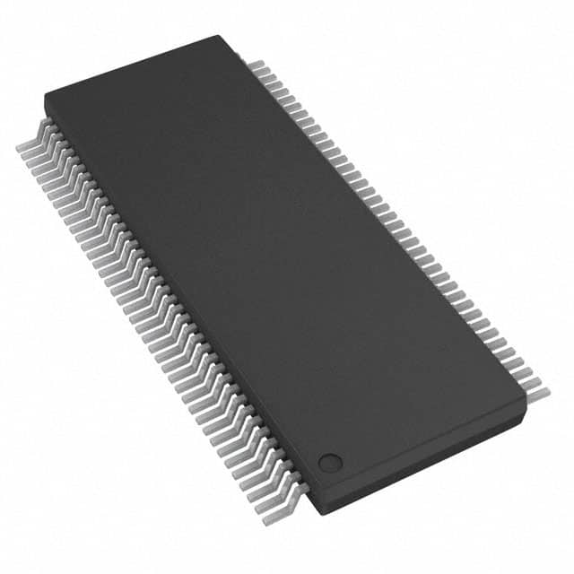
The 74ALVCH16831DBBRG4 is available in a small-outline package (SOIC) with 56 pins. It is typically sold in reels, with each reel containing a specified quantity of ICs.
Essence
The essence of the 74ALVCH16831DBBRG4 lies in its ability to provide reliable and efficient data transmission and buffering capabilities within electronic systems.
Specifications
- Supply voltage range: 1.65V to 3.6V
- Input/output voltage range: 0V to VCC
- Operating temperature range: -40°C to +85°C
- Output drive capability: ±24mA
- Propagation delay: 2.5ns (max)
- Input capacitance: 4pF (typ)
Detailed Pin Configuration
The 74ALVCH16831DBBRG4 has a total of 56 pins, each serving a specific function. The pin configuration is as follows:
- Pin 1: Output Enable (OE) for Channel A
- Pin 2: Data Input/Output (DQ0) for Channel A
- Pin 3: Data Input/Output (DQ1) for Channel A
- Pin 4: Data Input/Output (DQ2) for Channel A
- Pin 5: Data Input/Output (DQ3) for Channel A
- Pin 6: Data Input/Output (DQ4) for Channel A
- Pin 7: Data Input/Output (DQ5) for Channel A
- Pin 8: Data Input/Output (DQ6) for Channel A
- Pin 9: Data Input/Output (DQ7) for Channel A
- Pin 10: Data Input/Output (DQ8) for Channel A
- Pin 11: Data Input/Output (DQ9) for Channel A
- Pin 12: Data Input/Output (DQ10) for Channel A
- Pin 13: Data Input/Output (DQ11) for Channel A
- Pin 14: Data Input/Output (DQ12) for Channel A
- Pin 15: Data Input/Output (DQ13) for Channel A
- Pin 16: Data Input/Output (DQ14) for Channel A
- Pin 17: Data Input/Output (DQ15) for Channel A
- Pin 18: Data Input/Output (DQ16) for Channel A
- Pin 19: Data Input/Output (DQ17) for Channel A
- Pin 20: VCC (Positive Power Supply)
- Pin 21: Ground (GND)
- Pin 22: Output Enable (OE) for Channel B
- Pin 23: Data Input/Output (DQ0) for Channel B
- Pin 24: Data Input/Output (DQ1) for Channel B
- Pin 25: Data Input/Output (DQ2) for Channel B
- Pin 26: Data Input/Output (DQ3) for Channel B
- Pin 27: Data Input/Output (DQ4) for Channel B
- Pin 28: Data Input/Output (DQ5) for Channel B
- Pin 29: Data Input/Output (DQ6) for Channel B
- Pin 30: Data Input/Output (DQ7) for Channel B
- Pin 31: Data Input/Output (DQ8) for Channel B
- Pin 32: Data Input/Output (DQ9) for Channel B
- Pin 33
قم بإدراج 10 أسئلة وإجابات شائعة تتعلق بتطبيق 74ALVCH16831DBBRG4 في الحلول التقنية
Sure! Here are 10 common questions and answers related to the application of 74ALVCH16831DBBRG4 in technical solutions:
Q: What is the function of the 74ALVCH16831DBBRG4? A: The 74ALVCH16831DBBRG4 is a 18-bit universal bus driver with 3-state outputs, designed for high-speed CMOS applications.
Q: What is the operating voltage range of the 74ALVCH16831DBBRG4? A: The 74ALVCH16831DBBRG4 operates within a voltage range of 1.65V to 3.6V.
Q: Can the 74ALVCH16831DBBRG4 be used in both input and output applications? A: Yes, the 74ALVCH16831DBBRG4 can be used as both an input buffer and an output driver.
Q: What is the maximum data rate supported by the 74ALVCH16831DBBRG4? A: The 74ALVCH16831DBBRG4 supports a maximum data rate of 400 Mbps.
Q: Does the 74ALVCH16831DBBRG4 have built-in ESD protection? A: Yes, the 74ALVCH16831DBBRG4 has built-in ESD protection, making it suitable for robust applications.
Q: Can the 74ALVCH16831DBBRG4 drive multiple loads simultaneously? A: Yes, the 74ALVCH16831DBBRG4 can drive multiple loads simultaneously due to its 3-state outputs.
Q: What is the power supply current consumption of the 74ALVCH16831DBBRG4? A: The power supply current consumption of the 74ALVCH16831DBBRG4 is typically very low, making it energy-efficient.
Q: Is the 74ALVCH16831DBBRG4 compatible with other logic families? A: Yes, the 74ALVCH16831DBBRG4 is compatible with both TTL and CMOS logic families.
Q: Can the 74ALVCH16831DBBRG4 be used in high-speed data transmission applications? A: Yes, the 74ALVCH16831DBBRG4 is designed for high-speed CMOS applications, including data transmission.
Q: What is the package type of the 74ALVCH16831DBBRG4? A: The 74ALVCH16831DBBRG4 is available in a TSSOP (Thin Shrink Small Outline Package) package type.
Please note that these answers are general and may vary depending on specific application requirements.