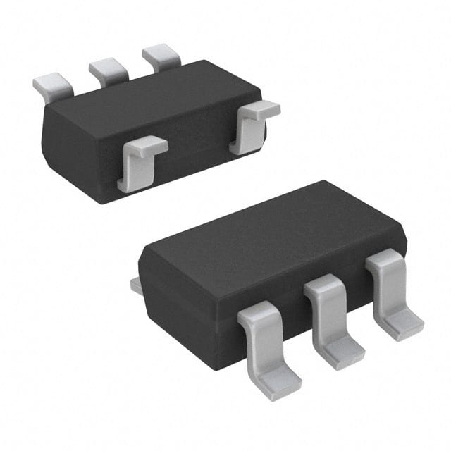
Encyclopedia Entry: 74LVC1G126DCKTG4
Product Overview
Category
The 74LVC1G126DCKTG4 belongs to the category of integrated circuits (ICs), specifically a single bus buffer gate.
Use
This IC is commonly used as a voltage level translator and buffer in various electronic devices and systems.
Characteristics
- Low-voltage CMOS technology
- High-speed operation
- Wide operating voltage range
- Schmitt-trigger action on inputs
- Balanced propagation delays
- Low power consumption
- Small package size
Package and Quantity
The 74LVC1G126DCKTG4 is available in a small SOT-23-5 package. It is typically sold in reels or tubes, with a quantity of 3000 units per reel.
Specifications
- Supply Voltage Range: 1.65V to 5.5V
- Input Voltage Range: GND to VCC
- Output Voltage Range: GND to VCC
- Maximum Operating Frequency: 400 MHz
- Input Capacitance: 3.5 pF
- Output Capacitance: 3.5 pF
- Operating Temperature Range: -40°C to +125°C
Pin Configuration
The 74LVC1G126DCKTG4 has a total of five pins:
- GND: Ground reference for the IC.
- A: Input pin for the data signal.
- OE: Output enable pin to control the output buffer.
- Y: Output pin for the translated/boosted signal.
- VCC: Power supply input for the IC.
Functional Features
- Voltage Level Translation: The IC can translate low-level signals to higher-level signals or vice versa, enabling compatibility between different voltage domains.
- Buffering: It provides buffering capabilities to ensure signal integrity and prevent signal degradation.
- Schmitt-trigger Action: The Schmitt-trigger inputs allow for noise immunity and hysteresis, enhancing the robustness of the IC.
Advantages and Disadvantages
Advantages
- Wide operating voltage range allows compatibility with various systems.
- High-speed operation enables efficient signal processing.
- Low power consumption contributes to energy efficiency.
- Small package size saves board space in compact designs.
Disadvantages
- Limited number of input/output pins restricts the complexity of applications.
- Not suitable for high-power applications due to its low current handling capability.
Working Principles
The 74LVC1G126DCKTG4 operates based on CMOS technology. It utilizes a combination of transistors to perform voltage level translation and buffering functions. When an input signal is applied, the IC amplifies and translates it to the desired output voltage level, ensuring proper signal propagation.
Application Field Plans
The 74LVC1G126DCKTG4 finds applications in various electronic systems, including but not limited to: - Mobile devices - Consumer electronics - Industrial automation - Automotive electronics - Communication systems
Alternative Models
Several alternative models can be considered as substitutes for the 74LVC1G126DCKTG4, depending on specific requirements and constraints. Some notable alternatives include: - SN74LVC1G126DBVR - MC74VHC1G126DTT1G - TC7SZ126FU
These alternatives offer similar functionality and characteristics, providing flexibility in choosing the most suitable option for a particular application.
In conclusion, the 74LVC1G126DCKTG4 is a versatile integrated circuit that serves as a voltage level translator and buffer. Its wide operating voltage range, high-speed operation, and small package size make it suitable for various electronic applications. While it has limitations in terms of pin count and current handling, alternative models offer flexibility for specific requirements.
قم بإدراج 10 أسئلة وإجابات شائعة تتعلق بتطبيق 74LVC1G126DCKTG4 في الحلول التقنية
Sure! Here are 10 common questions and answers related to the application of 74LVC1G126DCKTG4 in technical solutions:
Q1: What is the 74LVC1G126DCKTG4? A1: The 74LVC1G126DCKTG4 is a single bus buffer gate with 3-state output, designed for low-voltage (1.65V to 5.5V) applications.
Q2: What is the purpose of the 74LVC1G126DCKTG4? A2: The purpose of this IC is to provide buffering and level shifting capabilities in digital circuits.
Q3: What are the key features of the 74LVC1G126DCKTG4? A3: Some key features include high-speed operation, wide voltage range, 3-state outputs, and compatibility with various logic families.
Q4: How does the 74LVC1G126DCKTG4 work? A4: It acts as a buffer, taking an input signal and providing an amplified output signal with the same logic level.
Q5: What is the maximum operating frequency of the 74LVC1G126DCKTG4? A5: The maximum operating frequency is typically around 500 MHz.
Q6: Can the 74LVC1G126DCKTG4 be used in both digital and analog circuits? A6: No, it is primarily designed for digital applications and may not perform optimally in analog circuits.
Q7: What is the power supply voltage range for the 74LVC1G126DCKTG4? A7: The power supply voltage range is from 1.65V to 5.5V.
Q8: Can the 74LVC1G126DCKTG4 handle bidirectional signals? A8: No, it is a unidirectional buffer and cannot handle bidirectional signals.
Q9: What is the output drive strength of the 74LVC1G126DCKTG4? A9: The output drive strength is typically around 32 mA.
Q10: Can the 74LVC1G126DCKTG4 be used in automotive applications? A10: Yes, it is suitable for automotive applications as it can operate within the required voltage range and temperature specifications.
Please note that these answers are general and may vary depending on specific datasheet information and application requirements.


