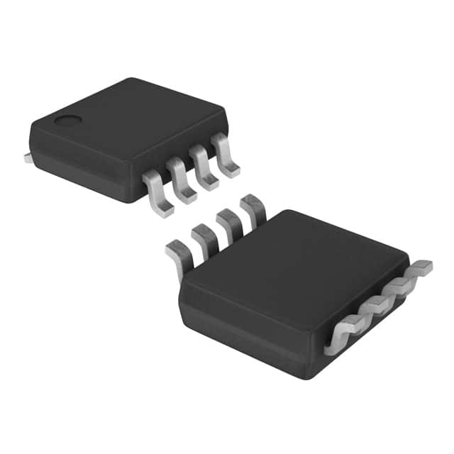
74LVC2G132DCUTE4
Basic Information Overview
- Category: Integrated Circuit (IC)
- Use: Logic Gate
- Characteristics: Low-voltage, high-speed, dual-input NAND Schmitt trigger gate
- Package: SOT353 (Ultra-Thin Small Outline Package)
- Essence: Digital logic gate for signal processing and control applications
- Packaging/Quantity: Tape and Reel, 3000 units per reel
Specifications
- Supply Voltage Range: 1.65V to 5.5V
- Input Voltage Range: -0.5V to VCC + 0.5V
- Output Voltage Range: 0V to VCC
- Operating Temperature Range: -40°C to +125°C
- Propagation Delay: 3.9ns (typical) at 3.3V supply voltage
- Input Capacitance: 3pF (typical)
Detailed Pin Configuration
The 74LVC2G132DCUTE4 has a total of 6 pins: 1. Pin 1: A Input (NAND Gate 1) 2. Pin 2: B Input (NAND Gate 1) 3. Pin 3: Y Output (NAND Gate 1) 4. Pin 4: A Input (NAND Gate 2) 5. Pin 5: B Input (NAND Gate 2) 6. Pin 6: Y Output (NAND Gate 2)
Functional Features
- Dual-input NAND Schmitt trigger gates provide hysteresis for improved noise immunity.
- High-speed operation allows for efficient signal processing.
- Low-voltage capability makes it suitable for battery-powered devices.
- Schmitt trigger inputs allow for easy interfacing with both digital and analog signals.
Advantages
- Compact SOT353 package enables space-saving designs.
- Wide supply voltage range allows for compatibility with various systems.
- Low power consumption enhances energy efficiency.
- Schmitt trigger inputs provide robust noise immunity.
Disadvantages
- Limited number of gates in a single package may restrict complex circuit designs.
- Propagation delay may affect timing-sensitive applications.
- SOT353 package may require specialized handling during assembly.
Working Principles
The 74LVC2G132DCUTE4 is based on CMOS technology, which utilizes complementary pairs of MOS transistors to implement logic functions. The NAND gate configuration consists of two inputs and one output. The Schmitt trigger feature ensures that the output transitions occur at different voltage levels for rising and falling input signals, providing noise immunity and signal conditioning.
Detailed Application Field Plans
The 74LVC2G132DCUTE4 finds applications in various fields, including: 1. Consumer Electronics: Used in smartphones, tablets, and portable devices for signal processing and control. 2. Industrial Automation: Employed in control systems and PLCs for logic operations. 3. Automotive Electronics: Integrated into automotive modules for reliable signal processing. 4. Communication Systems: Utilized in networking equipment and data transmission circuits.
Detailed and Complete Alternative Models
- 74LVC2G00DCUTG4: Dual 2-Input NAND Gate, SOT353 Package
- 74LVC2G08DCUTG4: Dual 2-Input AND Gate, SOT353 Package
- 74LVC2G86DCUTG4: Dual 2-Input XOR Gate, SOT353 Package
- 74LVC2G125DCUTG4: Dual Bus Buffer Gate, SOT353 Package
These alternative models offer similar functionality and are available in the same SOT353 package, providing flexibility in design choices.
In conclusion, the 74LVC2G132DCUTE4 is a low-voltage, high-speed dual-input NAND Schmitt trigger gate. Its compact package, wide supply voltage range, and noise immunity make it suitable for various applications in consumer electronics, industrial automation, automotive electronics, and communication systems. While it has limitations in terms of gate count and propagation delay, alternative models with similar functionality are available.
قم بإدراج 10 أسئلة وإجابات شائعة تتعلق بتطبيق 74LVC2G132DCUTE4 في الحلول التقنية
Sure! Here are 10 common questions and answers related to the application of 74LVC2G132DCUTE4 in technical solutions:
Q: What is the 74LVC2G132DCUTE4? A: The 74LVC2G132DCUTE4 is a dual 2-input NAND gate IC (integrated circuit) that operates at low voltage levels.
Q: What is the operating voltage range of the 74LVC2G132DCUTE4? A: The operating voltage range of the 74LVC2G132DCUTE4 is typically between 1.65V and 5.5V.
Q: What is the maximum output current of the 74LVC2G132DCUTE4? A: The maximum output current of the 74LVC2G132DCUTE4 is around 32mA.
Q: Can the 74LVC2G132DCUTE4 be used in battery-powered applications? A: Yes, the 74LVC2G132DCUTE4 can be used in battery-powered applications due to its low voltage operation.
Q: What is the propagation delay of the 74LVC2G132DCUTE4? A: The propagation delay of the 74LVC2G132DCUTE4 is typically around 4.3ns.
Q: Is the 74LVC2G132DCUTE4 suitable for high-speed applications? A: Yes, the 74LVC2G132DCUTE4 is designed for high-speed operation, making it suitable for various applications.
Q: Can the 74LVC2G132DCUTE4 handle both digital and analog signals? A: No, the 74LVC2G132DCUTE4 is primarily designed for digital signal processing and may not be suitable for analog signals.
Q: What is the package type of the 74LVC2G132DCUTE4? A: The 74LVC2G132DCUTE4 comes in a small SOT-353 package.
Q: Can the 74LVC2G132DCUTE4 be used in automotive applications? A: Yes, the 74LVC2G132DCUTE4 is qualified for automotive applications and can withstand harsh operating conditions.
Q: Are there any recommended external components to use with the 74LVC2G132DCUTE4? A: It is generally recommended to use decoupling capacitors near the power supply pins of the IC to ensure stable operation.
Please note that these answers are general and may vary depending on specific datasheet specifications and application requirements.


