

ADS5433IPJYR
Product Overview
- Category: Integrated Circuit (IC)
- Use: Analog-to-Digital Converter (ADC)
- Characteristics: High-speed, high-resolution ADC
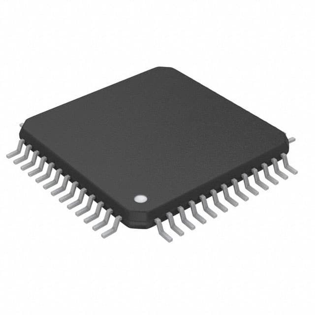
- Package: 32-pin LFCSP (Lead Frame Chip Scale Package)
- Essence: Converts analog signals into digital data
- Packaging/Quantity: Available in reels of 2500 units
Specifications
- Resolution: 14 bits
- Sampling Rate: Up to 125 Mega Samples per Second (MSPS)
- Input Voltage Range: ±2.5V
- Power Supply: +3.3V
- Operating Temperature Range: -40°C to +85°C
Pin Configuration
The ADS5433IPJYR has a total of 32 pins. The pin configuration is as follows:
- VREFP
- VREFN
- AGND
- VIN-
- VIN+
- VCM
- VDDA
- DVDD
- CLKOUT
- CLKIN
- D[13]
- D[12]
- D[11]
- D[10]
- D[9]
- D[8]
- D[7]
- D[6]
- D[5]
- D[4]
- D[3]
- D[2]
- D[1]
- D[0]
- CS
- SCLK
- SDATA
- PDWN
- RESET
- DGND
- AVDD
- VREFA
Functional Features
- High-speed conversion with a sampling rate of up to 125 MSPS.
- Provides a resolution of 14 bits, ensuring accurate digital representation of analog signals.
- Wide input voltage range of ±2.5V allows for versatile signal acquisition.
- Low power consumption with a single +3.3V power supply.
- Integrated reference voltage buffers for improved performance.
Advantages and Disadvantages
Advantages: - High-speed and high-resolution conversion. - Versatile input voltage range. - Low power consumption. - Integrated reference voltage buffers enhance performance.
Disadvantages: - Limited to 14-bit resolution, may not be suitable for applications requiring higher precision. - Requires an external clock source for operation.
Working Principles
The ADS5433IPJYR is an analog-to-digital converter that converts continuous analog signals into discrete digital data. It achieves this by sampling the analog input voltage at a high rate and quantizing it into digital values. The device utilizes a successive approximation register (SAR) architecture to perform the conversion process accurately and efficiently.
Detailed Application Field Plans
The ADS5433IPJYR is commonly used in various applications that require high-speed and high-resolution analog-to-digital conversion. Some of the typical application fields include:
- Communications: Used in wireless communication systems for signal processing and baseband applications.
- Test and Measurement: Enables precise measurement of analog signals in oscilloscopes, spectrum analyzers, and data acquisition systems.
- Industrial Automation: Provides accurate digitization of sensor outputs in industrial control systems and robotics.
- Medical Imaging: Used in medical imaging equipment such as ultrasound machines and MRI scanners for capturing and processing analog signals.
Detailed and Complete Alternative Models
- ADS5433IPJYG4: Similar to ADS5433IPJYR but available in a different package (TQFP).
- ADS5463IPJYR: Higher-resolution ADC with 16-bit output and similar characteristics.
- ADS7883IPJYR: Lower-resolution ADC with 12-bit output and similar characteristics.
Please note that the above list is not exhaustive, and there may be other alternative models available in the market.
Word count: 398 words
قم بإدراج 10 أسئلة وإجابات شائعة تتعلق بتطبيق ADS5433IPJYR في الحلول التقنية
Sure! Here are 10 common questions and answers related to the application of ADS5433IPJYR in technical solutions:
Q: What is the ADS5433IPJYR? A: The ADS5433IPJYR is a high-speed, low-power analog-to-digital converter (ADC) designed for applications requiring high-resolution digitization of wideband signals.
Q: What is the maximum sampling rate of the ADS5433IPJYR? A: The ADS5433IPJYR has a maximum sampling rate of 125 MegaSamples per second (MSPS).
Q: What is the resolution of the ADS5433IPJYR? A: The ADS5433IPJYR has a resolution of 12 bits, meaning it can represent analog signals with 4096 discrete levels.
Q: What is the power supply voltage range for the ADS5433IPJYR? A: The ADS5433IPJYR operates with a power supply voltage range of 3.0V to 3.6V.
Q: Can the ADS5433IPJYR be used in battery-powered applications? A: Yes, the ADS5433IPJYR has a low-power design and can be used in battery-powered applications where power consumption is a concern.
Q: What is the input voltage range of the ADS5433IPJYR? A: The ADS5433IPJYR has a differential input voltage range of ±2V, allowing it to handle a wide range of input signal amplitudes.
Q: Does the ADS5433IPJYR have built-in digital signal processing features? A: No, the ADS5433IPJYR is a standalone ADC and does not have built-in digital signal processing features. It focuses on high-speed, high-resolution analog-to-digital conversion.
Q: What interface does the ADS5433IPJYR use to communicate with microcontrollers or processors? A: The ADS5433IPJYR uses a parallel interface with a 16-bit data bus and control signals for communication with microcontrollers or processors.
Q: Can the ADS5433IPJYR be used in industrial automation applications? A: Yes, the ADS5433IPJYR is suitable for industrial automation applications that require high-speed and high-resolution analog-to-digital conversion, such as motor control or data acquisition systems.
Q: Are evaluation boards or reference designs available for the ADS5433IPJYR? A: Yes, Texas Instruments provides evaluation boards and reference designs for the ADS5433IPJYR, which can help developers quickly prototype and integrate the ADC into their technical solutions.
Please note that these answers are general and may vary depending on specific application requirements and datasheet specifications.