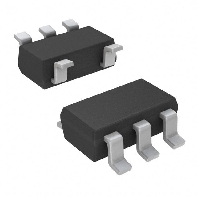
CLVC1G125IDCKREP
Product Overview
- Category: Integrated Circuit (IC)
- Use: Logic Level Shifter
- Characteristics: Single Gate, Non-Inverting, 3-State Output
- Package: SC-70-5
- Essence: This IC is designed to shift logic levels between different voltage domains in electronic circuits.
- Packaging/Quantity: Available in tape and reel packaging, with a quantity of 3000 units per reel.
Specifications
- Supply Voltage Range: 1.65V to 5.5V
- High-Level Input Voltage: 2.3V to VCC
- Low-Level Input Voltage: GND to 0.8V
- High-Level Output Voltage: 2.4V to VCC
- Low-Level Output Voltage: GND to 0.4V
- Maximum Propagation Delay Time: 6.5ns
- Maximum Operating Frequency: 200MHz
Detailed Pin Configuration
The CLVC1G125IDCKREP has the following pin configuration:
- Pin 1: A - Input
- Pin 2: OE - Output Enable
- Pin 3: Y - Output
- Pin 4: VCC - Power Supply
- Pin 5: GND - Ground
Functional Features
- Logic Level Shifting: The CLVC1G125IDCKREP allows for seamless shifting of logic levels between different voltage domains, enabling communication between devices operating at different voltage levels.
- Non-Inverting Operation: The input signal is not inverted at the output, maintaining the same logic state.
- 3-State Output: The output can be put into a high-impedance state using the OE pin, allowing multiple devices to share a common bus.
Advantages and Disadvantages
Advantages: - Wide supply voltage range allows compatibility with various systems. - Fast propagation delay time enables high-speed data transmission. - Small package size (SC-70-5) saves board space.
Disadvantages: - Limited output current capability may restrict use in certain applications. - Single gate design may not be suitable for complex logic operations.
Working Principles
The CLVC1G125IDCKREP utilizes a combination of MOSFETs and CMOS technology to achieve logic level shifting. The input signal is passed through a level shifter circuit, which adjusts the voltage levels according to the specified supply voltage range. The non-inverting characteristic ensures that the output signal maintains the same logic state as the input.
Detailed Application Field Plans
The CLVC1G125IDCKREP can be used in various applications, including:
- Battery-Powered Devices: It allows for communication between low-voltage microcontrollers and higher voltage peripherals, extending battery life.
- Sensor Interfaces: It facilitates interfacing between sensors operating at different voltage levels and microcontrollers or processing units.
- Communication Systems: It enables level shifting between different communication protocols, such as UART, I2C, SPI, etc., ensuring compatibility between devices.
- Industrial Control Systems: It can be utilized in control systems where different components operate at different voltage levels, enabling seamless integration.
Detailed and Complete Alternative Models
- SN74LVC1G125DBVR: Single Gate Non-Inverting 3-State Output Logic Level Shifter, SOT-23-5 package.
- NC7SZ125P5X: Single Gate Non-Inverting 3-State Output Logic Level Shifter, SC-70-5 package.
- MC74VHC1GT125DF1G: Single Gate Non-Inverting 3-State Output Logic Level Shifter, SOT-353 package.
These alternative models provide similar functionality and can be considered as alternatives to the CLVC1G125IDCKREP.
Word count: 443 words
قم بإدراج 10 أسئلة وإجابات شائعة تتعلق بتطبيق CLVC1G125IDCKREP في الحلول التقنية
Sure! Here are 10 common questions and answers related to the application of CLVC1G125IDCKREP in technical solutions:
Q1: What is CLVC1G125IDCKREP? A1: CLVC1G125IDCKREP is a specific integrated circuit (IC) that belongs to the CLVC family. It is a single bus buffer gate with 3-state output, designed for voltage level translation applications.
Q2: What is the voltage range supported by CLVC1G125IDCKREP? A2: CLVC1G125IDCKREP supports a voltage range from 1.65V to 5.5V, making it compatible with various logic families.
Q3: What is the maximum data rate supported by CLVC1G125IDCKREP? A3: CLVC1G125IDCKREP can support data rates up to 400 Mbps, making it suitable for high-speed applications.
Q4: Can CLVC1G125IDCKREP be used as a bidirectional buffer? A4: No, CLVC1G125IDCKREP is a unidirectional buffer and does not support bidirectional communication.
Q5: How many inputs and outputs does CLVC1G125IDCKREP have? A5: CLVC1G125IDCKREP has one input and one output.
Q6: Is CLVC1G125IDCKREP capable of driving capacitive loads? A6: Yes, CLVC1G125IDCKREP can drive capacitive loads up to 50 pF.
Q7: Can CLVC1G125IDCKREP be used in mixed-voltage level translation applications? A7: Yes, CLVC1G125IDCKREP is commonly used for mixed-voltage level translation between different logic families.
Q8: What is the power supply voltage range for CLVC1G125IDCKREP? A8: The power supply voltage range for CLVC1G125IDCKREP is from 1.65V to 5.5V.
Q9: Does CLVC1G125IDCKREP have built-in ESD protection? A9: Yes, CLVC1G125IDCKREP has built-in ESD protection, which helps safeguard against electrostatic discharge events.
Q10: Is CLVC1G125IDCKREP available in different package options? A10: Yes, CLVC1G125IDCKREP is available in various package options, such as SC-70 and VSSOP, providing flexibility for different design requirements.
Please note that these answers are general and may vary depending on the specific datasheet and manufacturer's specifications of CLVC1G125IDCKREP.


