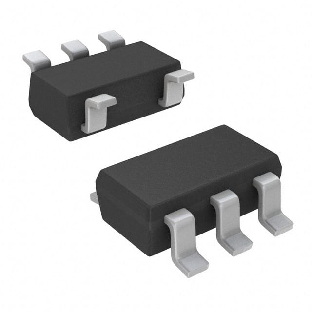
CLVC1G32MDCKREPG4
Basic Information Overview
- Category: Integrated Circuit (IC)
- Use: Logic Gate
- Characteristics: Single 2-Input OR Gate
- Package: MDCK (MicroDFN)
- Essence: High-Speed CMOS Logic
- Packaging/Quantity: Tape and Reel, 3000 pieces per reel
Specifications
- Supply Voltage Range: 1.65V to 5.5V
- Input Voltage Range: -0.5V to VCC + 0.5V
- Output Voltage Range: 0V to VCC
- Operating Temperature Range: -40°C to +85°C
- Propagation Delay: 3.6ns (typical) at 3.3V
- Maximum Quiescent Current: 10μA at 5.5V
Detailed Pin Configuration
The CLVC1G32MDCKREPG4 has a total of 5 pins: 1. Pin 1: Input A 2. Pin 2: Input B 3. Pin 3: Ground (GND) 4. Pin 4: Output Y 5. Pin 5: Power Supply (VCC)
Functional Features
- High-Speed Operation: The CLVC1G32MDCKREPG4 is designed for high-speed logic applications, ensuring fast signal processing.
- Low Power Consumption: With a maximum quiescent current of only 10μA, this IC offers energy-efficient operation.
- Wide Voltage Range: The supply voltage range of 1.65V to 5.5V allows compatibility with various systems.
- ESD Protection: The device incorporates Electrostatic Discharge (ESD) protection, enhancing its reliability.
Advantages and Disadvantages
Advantages: - High-speed operation enables quick data processing. - Low power consumption contributes to energy efficiency. - Wide voltage range allows compatibility with different systems. - ESD protection enhances reliability.
Disadvantages: - Limited functionality: The CLVC1G32MDCKREPG4 is a single 2-input OR gate and may not be suitable for complex logic operations requiring multiple gates.
Working Principles
The CLVC1G32MDCKREPG4 operates based on Complementary Metal-Oxide-Semiconductor (CMOS) technology. It utilizes transistors to perform logical operations, specifically an OR gate in this case. When both input A and input B are low (0V), the output Y will also be low. If either input A or input B (or both) is high (VCC), the output Y will be high.
Detailed Application Field Plans
The CLVC1G32MDCKREPG4 can be used in various applications, including but not limited to: - Digital signal processing - Data communication systems - Microcontrollers - Computer peripherals - Industrial automation
Detailed and Complete Alternative Models
- SN74LVC1G32DBVR: Single 2-Input OR Gate, SOT-23 package
- MC74VHC1G32DTT1G: Single 2-Input OR Gate, SOT-23-5 package
- CD4011BE: Quad 2-Input NAND Gate, DIP-14 package
- 74HC08D: Quad 2-Input AND Gate, SOIC-14 package
- CD4073BNSR: Triple 3-Input AND Gate, SOP-14 package
(Note: The above list provides alternative models with different functionalities and packages.)
This entry provides an overview of the CLVC1G32MDCKREPG4, a single 2-input OR gate integrated circuit. It includes basic information, specifications, pin configuration, functional features, advantages and disadvantages, working principles, application field plans, and alternative models.
قم بإدراج 10 أسئلة وإجابات شائعة تتعلق بتطبيق CLVC1G32MDCKREPG4 في الحلول التقنية
Question: What is CLVC1G32MDCKREPG4?
Answer: CLVC1G32MDCKREPG4 is a specific type of logic gate, specifically a single 2-input OR gate, that is commonly used in technical solutions.Question: What is the purpose of using CLVC1G32MDCKREPG4 in technical solutions?
Answer: The purpose of using CLVC1G32MDCKREPG4 is to perform logical operations, specifically the OR operation, in electronic circuits or systems.Question: What are the key features of CLVC1G32MDCKREPG4?
Answer: Some key features of CLVC1G32MDCKREPG4 include low power consumption, high-speed operation, and compatibility with various voltage levels.Question: How does CLVC1G32MDCKREPG4 work?
Answer: CLVC1G32MDCKREPG4 works by taking two input signals and producing an output signal based on the logical OR operation between the inputs.Question: What is the voltage range supported by CLVC1G32MDCKREPG4?
Answer: CLVC1G32MDCKREPG4 supports a wide voltage range, typically from 1.65V to 5.5V, making it compatible with various voltage levels in different applications.Question: Can CLVC1G32MDCKREPG4 be used in battery-powered devices?
Answer: Yes, CLVC1G32MDCKREPG4 is suitable for battery-powered devices due to its low power consumption, making it an energy-efficient choice.Question: Is CLVC1G32MDCKREPG4 compatible with other logic gates?
Answer: Yes, CLVC1G32MDCKREPG4 is compatible with other logic gates, allowing it to be integrated into larger logic circuits or systems.Question: What are some typical applications of CLVC1G32MDCKREPG4?
Answer: Some typical applications of CLVC1G32MDCKREPG4 include signal conditioning, data processing, digital communication systems, and control systems.Question: Can CLVC1G32MDCKREPG4 be used in high-speed applications?
Answer: Yes, CLVC1G32MDCKREPG4 is designed for high-speed operation, making it suitable for applications that require fast response times.Question: Where can I find more information about CLVC1G32MDCKREPG4?
Answer: More information about CLVC1G32MDCKREPG4 can be found in the datasheet provided by the manufacturer or by consulting technical resources related to logic gates and digital electronics.


