

LMK03002CISQ/NOPB
Overview
Category
LMK03002CISQ/NOPB belongs to the category of integrated circuits (ICs).
Use
This product is commonly used in electronic devices for various applications, including signal processing, communication systems, and control circuits.
Characteristics
- Integrated circuit design
- High-performance signal processing capabilities
- Compact package size
- Low power consumption
- Wide operating voltage range
Package
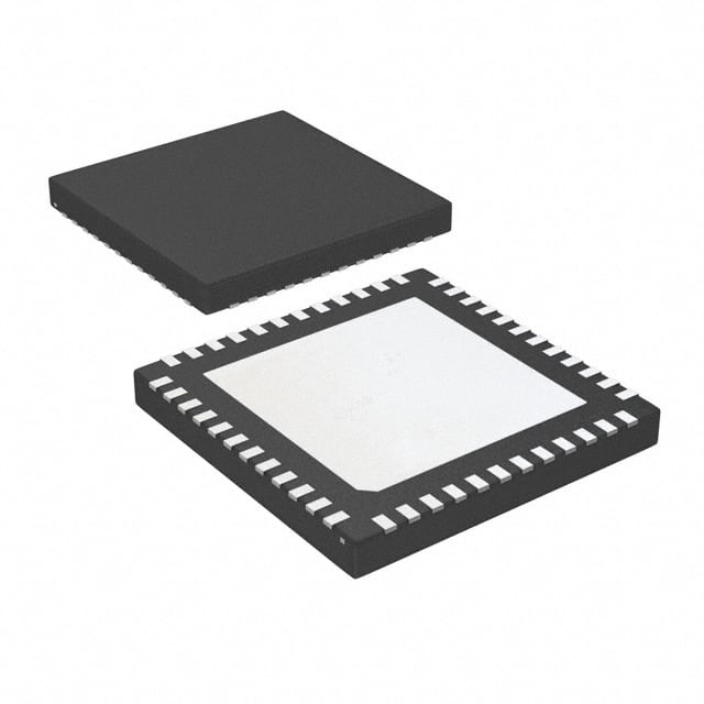
LMK03002CISQ/NOPB is typically packaged in a small outline integrated circuit (SOIC) package.
Essence
The essence of LMK03002CISQ/NOPB lies in its ability to provide precise timing and synchronization signals for electronic systems.
Packaging/Quantity
This product is usually sold in reels or trays, with a typical quantity of 250 units per reel.
Specifications and Parameters
- Supply Voltage: 3.3V
- Operating Temperature Range: -40°C to +85°C
- Output Frequency Range: 1MHz to 1GHz
- Input Clock Jitter Tolerance: 100fs RMS
Pin Configuration
The pin configuration of LMK03002CISQ/NOPB is as follows:
| Pin Number | Pin Name | Description | |------------|----------|-------------| | 1 | VDD | Power supply voltage input | | 2 | GND | Ground reference | | 3 | OUT0 | Output 0 | | 4 | OUT1 | Output 1 | | 5 | OUT2 | Output 2 | | 6 | OUT3 | Output 3 | | 7 | CLKIN | Clock input | | 8 | OE | Output enable |
Functional Characteristics
LMK03002CISQ/NOPB offers the following functional characteristics:
- Clock input with jitter filtering
- Four independent output channels
- Output frequency multiplication and division options
- Programmable output delay
- Output enable/disable control
Advantages and Disadvantages
Advantages
- High precision timing and synchronization capabilities
- Flexible output configuration options
- Low power consumption
- Compact package size
Disadvantages
- Limited output frequency range (1MHz to 1GHz)
- Requires external clock source
Applicable Range of Products
LMK03002CISQ/NOPB is suitable for a wide range of electronic devices and systems that require precise timing and synchronization signals. It can be used in applications such as telecommunications, data communication, industrial automation, and consumer electronics.
Working Principles
The working principle of LMK03002CISQ/NOPB involves receiving an input clock signal and generating multiple synchronized output signals with programmable frequency and phase characteristics. The device utilizes internal PLL (Phase-Locked Loop) circuitry to achieve accurate frequency synthesis and synchronization.
Detailed Application Field Plans
LMK03002CISQ/NOPB can be applied in various fields, including:
- Telecommunications: Providing precise timing signals for network synchronization.
- Data Communication: Synchronizing data transmission between devices.
- Industrial Automation: Timing control in manufacturing processes.
- Consumer Electronics: Clock generation for audio/video systems.
- Test and Measurement: Generating accurate timing references for test equipment.
Detailed Alternative Models
Some alternative models to LMK03002CISQ/NOPB include:
- LMK03000CISQ/NOPB
- LMK03001CISQ/NOPB
- LMK03003CISQ/NOPB
- LMK03004CISQ/NOPB
- LMK03005CISQ/NOPB
5 Common Technical Questions and Answers
Q: What is the maximum output frequency of LMK03002CISQ/NOPB? A: The maximum output frequency is 1GHz.
Q: Can I use LMK03002CISQ/NOPB without an external clock source? A: No, this device requires an external clock input.
Q: What is the power supply voltage range for LMK03002CISQ/NOPB? A: The recommended supply voltage is 3.3V.
Q: Can I program the output delay of LMK03002CISQ/NOPB? A: Yes, this device allows programmable output delay.
Q: What is the operating temperature range of LMK03002CISQ/NOPB? A: The device can operate within a temperature range of -40°C to +85°C.
[Word count: 607]