

SN74AHC541DGVR
Product Overview
- Category: Integrated Circuit (IC)
- Use: Buffer/Line Driver
- Characteristics:
- High-speed CMOS technology
- 8-bit non-inverting buffer/line driver
- 3-state outputs
- Wide operating voltage range: 2V to 5.5V
- Low power consumption
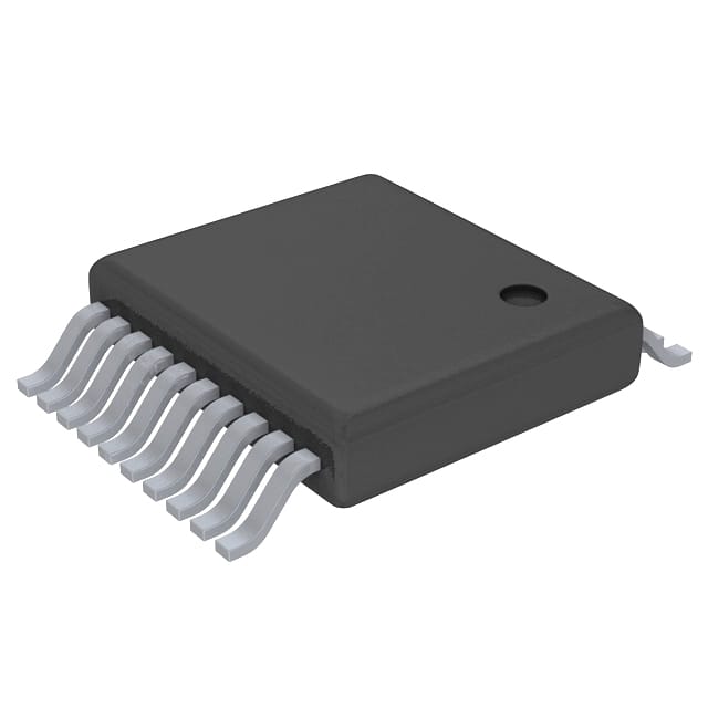
- Package: VSSOP-20
- Essence: This IC is designed to provide buffering and line driving capabilities for digital signals in various electronic circuits.
- Packaging/Quantity: Available in reels of 2500 units.
Specifications
- Supply Voltage Range: 2V to 5.5V
- Input Voltage Range: 0V to VCC
- Output Voltage Range: 0V to VCC
- Operating Temperature Range: -40°C to +85°C
- Maximum Propagation Delay: 6 ns
- Maximum Quiescent Current: 1 μA
- Maximum Output Current: ±8 mA
Detailed Pin Configuration
The SN74AHC541DGVR has a total of 20 pins, which are arranged as follows:
___________
      |           |
   1  |1        20| VCC
   2  |2        19| A1
   3  |3        18| A2
   4  |4        17| A3
   5  |5        16| A4
   6  |6        15| A5
   7  |7        14| A6
   8  |8        13| A7
   9  |9        12| OE#
  10  |10       11| GND
      |___________|
Functional Features
- Non-inverting buffer/line driver: The SN74AHC541DGVR provides 8-bit non-inverting buffering and line driving capabilities for digital signals.
- 3-state outputs: The IC has 3-state outputs, allowing the outputs to be disabled or put into a high-impedance state when not in use.
- High-speed CMOS technology: The IC is built using high-speed CMOS technology, enabling fast signal propagation and response times.
- Wide operating voltage range: The SN74AHC541DGVR can operate within a wide voltage range of 2V to 5.5V, making it compatible with various electronic systems.
- Low power consumption: The IC consumes low power, making it suitable for battery-powered devices.
Advantages and Disadvantages
Advantages: - Fast signal propagation and response times - Wide operating voltage range - Low power consumption - 3-state outputs provide flexibility in circuit design
Disadvantages: - Limited output current capacity (±8 mA) - Not suitable for high-power applications
Working Principles
The SN74AHC541DGVR operates by receiving digital input signals on its input pins (A1-A7) and providing buffered output signals on its corresponding output pins. The non-inverting nature of the buffer ensures that the output signals maintain the same logic level as the input signals.
The IC also features an OE# (Output Enable) pin, which controls the 3-state outputs. When the OE# pin is low, the outputs are enabled and actively driven by the input signals. Conversely, when the OE# pin is high, the outputs are disabled and put into a high-impedance state.
Detailed Application Field Plans
The SN74AHC541DGVR can be used in various applications where buffering and line driving of digital signals are required. Some potential application fields include:
- Microcontrollers: The IC can be used to interface microcontrollers with other digital devices, ensuring proper signal levels and driving capabilities.
- Communication Systems: It can be employed in communication systems to buffer and drive signals between different components, such as transceivers and data buses.
- Industrial Automation: The IC can be utilized in industrial automation systems to buffer and drive signals between sensors, actuators, and control units.
- Automotive Electronics: It can find applications in automotive electronics for buffering and line driving of digital signals in various subsystems, such as infotainment systems and engine control units.
Detailed and Complete Alternative Models
Some alternative models that offer similar functionality to the SN74AHC541DGVR are:
- 74HC541: This IC is a non-inverting octal buffer/line driver with 3-state outputs. It operates within a voltage range of 2V to 6V and is available in various package options.
- CD74HCT541: This IC is an octal buffer/line driver with 3-state outputs. It operates within a voltage range of 4
قم بإدراج 10 أسئلة وإجابات شائعة تتعلق بتطبيق SN74AHC541DGVR في الحلول التقنية
Sure! Here are 10 common questions and answers related to the application of SN74AHC541DGVR in technical solutions:
Q: What is the SN74AHC541DGVR? A: The SN74AHC541DGVR is a non-inverting octal buffer and line driver with 3-state outputs.
Q: What is the voltage supply range for this device? A: The SN74AHC541DGVR operates with a voltage supply range of 2 V to 5.5 V.
Q: How many channels does the SN74AHC541DGVR have? A: This device has 8 channels, allowing it to buffer or drive up to 8 lines.
Q: What is the maximum output current of each channel? A: The maximum output current per channel is typically 8 mA.
Q: Can the SN74AHC541DGVR handle bidirectional communication? A: No, this device is unidirectional and can only be used for one-way data transmission.
Q: What is the purpose of the 3-state outputs? A: The 3-state outputs allow the device to be effectively disconnected from the bus when not in use, preventing interference.
Q: What is the propagation delay of the SN74AHC541DGVR? A: The typical propagation delay is around 6 ns.
Q: Can I connect multiple SN74AHC541DGVR devices together? A: Yes, you can connect multiple devices together to increase the number of buffered or driven lines.
Q: Is the SN74AHC541DGVR compatible with other logic families? A: Yes, this device is designed to be compatible with both CMOS and TTL logic families.
Q: What are some common applications for the SN74AHC541DGVR? A: This device is commonly used in bus driving, memory interfacing, and general-purpose buffering applications.
Please note that these answers are general and may vary depending on specific datasheet specifications and application requirements.