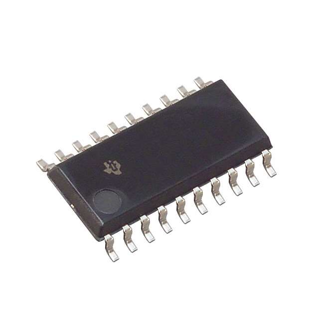
SN74AHCT541NSR
Product Overview
- Category: Integrated Circuit (IC)
- Use: Buffer/Line Driver
- Characteristics: High-speed, CMOS technology
- Package: SOIC (Small Outline Integrated Circuit)
- Essence: Non-inverting octal buffer/line driver with 3-state outputs
- Packaging/Quantity: Tape and Reel, 2500 pieces per reel
Specifications
- Supply Voltage Range: 4.5V to 5.5V
- Input Voltage Range: 0V to VCC
- Output Voltage Range: 0V to VCC
- Operating Temperature Range: -40°C to +85°C
- Propagation Delay Time: 6 ns (typical)
- Output Current: ±8 mA
- Input Capacitance: 3 pF (typical)
Detailed Pin Configuration
The SN74AHCT541NSR has a total of 20 pins, which are arranged as follows:
- OE (Output Enable) - Active Low
- A1 - Input A1
- Y1 - Output Y1
- A2 - Input A2
- Y2 - Output Y2
- A3 - Input A3
- Y3 - Output Y3
- GND (Ground)
- Y4 - Output Y4
- A4 - Input A4
- Y5 - Output Y5
- A5 - Input A5
- Y6 - Output Y6
- A6 - Input A6
- Y7 - Output Y7
- A7 - Input A7
- VCC (Supply Voltage)
- Y8 - Output Y8
- A8 - Input A8
- OE (Output Enable) - Active Low
Functional Features
- Non-inverting buffer/line driver
- 3-state outputs for bus-oriented applications
- High-speed operation with CMOS technology
- Low power consumption
- Schmitt-trigger inputs for noise immunity
- ESD protection on all inputs and outputs
Advantages and Disadvantages
Advantages: - High-speed operation allows for efficient data transfer - CMOS technology provides low power consumption - Schmitt-trigger inputs ensure reliable performance in noisy environments - ESD protection safeguards the IC from electrostatic discharge
Disadvantages: - Limited output current may restrict use in certain applications - Narrow supply voltage range may limit compatibility with other systems
Working Principles
The SN74AHCT541NSR is designed to act as a non-inverting buffer/line driver. It takes input signals and amplifies them to drive output lines. The 3-state outputs allow multiple devices to share a common bus, enabling bidirectional communication.
When the Output Enable (OE) pin is low, the outputs are enabled and reflect the input signals. Conversely, when OE is high, the outputs are in a high-impedance state, effectively disconnecting them from the bus.
Detailed Application Field Plans
The SN74AHCT541NSR is commonly used in various applications, including:
- Data communication systems
- Memory address decoding
- Bus interface between microcontrollers and peripherals
- Industrial control systems
- Automotive electronics
- Networking equipment
Detailed and Complete Alternative Models
- SN74AHCT540NSR: Octal buffer/line driver with inverting outputs
- SN74AHCT541DGV: Octal buffer/line driver in TSSOP package
- SN74AHCT541PWR: Octal buffer/line driver in TSSOP package with PowerPAD
These alternative models offer similar functionality to the SN74AHCT541NSR but may differ in package type, pin configuration, or other specifications.
In conclusion, the SN74AHCT541NSR is a high-speed non-inverting octal buffer/line driver with 3-state outputs. It is widely used in various applications due to its reliable performance, low power consumption, and compatibility with CMOS technology.
قم بإدراج 10 أسئلة وإجابات شائعة تتعلق بتطبيق SN74AHCT541NSR في الحلول التقنية
Sure! Here are 10 common questions and answers related to the application of SN74AHCT541NSR:
Q: What is SN74AHCT541NSR? A: SN74AHCT541NSR is a non-inverting octal buffer and line driver with 3-state outputs, commonly used in digital systems.
Q: What is the voltage supply range for SN74AHCT541NSR? A: The voltage supply range for SN74AHCT541NSR is typically between 4.5V and 5.5V.
Q: What is the maximum output current that SN74AHCT541NSR can drive? A: SN74AHCT541NSR can drive up to 8 mA of output current per channel.
Q: Can SN74AHCT541NSR be used as a level shifter? A: Yes, SN74AHCT541NSR can be used as a level shifter to convert signals between different voltage levels.
Q: How many input and output pins does SN74AHCT541NSR have? A: SN74AHCT541NSR has 8 input pins and 8 output pins.
Q: Is SN74AHCT541NSR compatible with TTL logic levels? A: Yes, SN74AHCT541NSR is compatible with both TTL and CMOS logic levels.
Q: Can SN74AHCT541NSR be used in bidirectional communication? A: No, SN74AHCT541NSR is a unidirectional buffer and line driver, not suitable for bidirectional communication.
Q: What is the purpose of the 3-state outputs in SN74AHCT541NSR? A: The 3-state outputs allow multiple devices to share a common bus without interfering with each other.
Q: Can SN74AHCT541NSR be used in high-speed applications? A: Yes, SN74AHCT541NSR has a maximum propagation delay of 10 ns, making it suitable for many high-speed applications.
Q: Are there any special considerations when using SN74AHCT541NSR in noisy environments? A: It is recommended to use decoupling capacitors near the power supply pins and proper grounding techniques to minimize noise interference.
Please note that these answers are general and may vary depending on specific application requirements.


