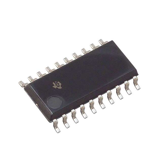
SN74ALVCH244NSR
Product Overview
- Category: Integrated Circuit (IC)
- Use: Buffer/Line Driver
- Characteristics: High-speed, low-voltage, non-inverting
- Package: 20-pin small-outline integrated circuit (SOIC)
- Essence: Logic level translator/buffer
- Packaging/Quantity: Tape and reel, 2500 units per reel
Specifications
- Supply Voltage Range: 1.65V to 3.6V
- Input Voltage Range: 0V to VCC
- Output Voltage Range: 0V to VCC
- Maximum Operating Frequency: 500 MHz
- Propagation Delay: 2.5 ns (typical)
- Output Drive Strength: ±24 mA
- ESD Protection: >2000V (Human Body Model)
Detailed Pin Configuration
The SN74ALVCH244NSR has a total of 20 pins, numbered as follows:
- A1
- Y1
- A2
- Y2
- A3
- Y3
- A4
- GND
- Y4
- OE#
- A5
- Y5
- A6
- Y6
- A7
- VCC
- Y7
- A8
- Y8
- A9
Functional Features
- Non-inverting buffer with 3-state outputs
- Supports bidirectional data flow
- Provides voltage level translation between different logic families
- High-speed operation suitable for high-frequency applications
- Low power consumption
- Schmitt-trigger inputs for noise immunity
Advantages and Disadvantages
Advantages: - Wide supply voltage range allows compatibility with various systems - High-speed operation enables efficient data transfer - 3-state outputs facilitate bus sharing and multiplexing - Schmitt-trigger inputs provide robustness against noise
Disadvantages: - Limited output drive strength may not be suitable for driving heavy loads - Not compatible with higher voltage logic families (e.g., TTL)
Working Principles
The SN74ALVCH244NSR is a non-inverting buffer that translates logic levels between different voltage domains. It operates by receiving input signals on the A1-A9 pins and providing corresponding output signals on the Y1-Y8 pins. The OE# pin controls the output enable/disable function.
When the OE# pin is low, the outputs are enabled and mirror the input signals. When the OE# pin is high, the outputs are in a high-impedance state, allowing other devices to drive the bus lines.
The device operates within a specified supply voltage range and provides fast propagation delay, making it suitable for high-speed applications.
Detailed Application Field Plans
The SN74ALVCH244NSR is commonly used in various digital systems where voltage level translation and buffering are required. Some typical application fields include:
- Microcontrollers and microprocessors
- Communication systems
- Data acquisition systems
- Industrial automation
- Automotive electronics
- Consumer electronics
In these applications, the SN74ALVCH244NSR helps interface different logic families operating at different voltage levels, ensuring proper signal integrity and reliable data transfer.
Detailed and Complete Alternative Models
- SN74LVC244A: Similar functionality but operates at a lower voltage range (1.65V to 3.6V)
- SN74LVCH244A: Higher drive strength variant of SN74ALVCH244NSR
- SN74HCT244: Compatible with TTL logic family, operates at higher voltage levels (4.5V to 5.5V)
- SN74LV1T244: Single-channel buffer with similar functionality, suitable for low-power applications
These alternative models offer different voltage ranges, drive strengths, and compatibility with other logic families, providing flexibility in selecting the most suitable device for specific requirements.
Word count: 526 words
قم بإدراج 10 أسئلة وإجابات شائعة تتعلق بتطبيق SN74ALVCH244NSR في الحلول التقنية
Sure! Here are 10 common questions and answers related to the application of SN74ALVCH244NSR:
Q: What is SN74ALVCH244NSR? A: SN74ALVCH244NSR is a non-inverting octal buffer and line driver with 3-state outputs, commonly used in digital logic applications.
Q: What is the voltage supply range for SN74ALVCH244NSR? A: The voltage supply range for SN74ALVCH244NSR is typically between 1.65V and 3.6V.
Q: What is the maximum output current that SN74ALVCH244NSR can drive? A: SN74ALVCH244NSR can typically drive up to 24mA of output current.
Q: Can SN74ALVCH244NSR be used as a level shifter? A: Yes, SN74ALVCH244NSR can be used as a level shifter to convert signals between different voltage levels.
Q: How many inputs and outputs does SN74ALVCH244NSR have? A: SN74ALVCH244NSR has 8 inputs and 8 outputs.
Q: What is the propagation delay of SN74ALVCH244NSR? A: The propagation delay of SN74ALVCH244NSR is typically around 2.7ns.
Q: Can SN74ALVCH244NSR be used in high-speed applications? A: Yes, SN74ALVCH244NSR is designed for high-speed operation and can be used in applications with fast switching requirements.
Q: Is SN74ALVCH244NSR compatible with other logic families? A: SN74ALVCH244NSR is compatible with a wide range of logic families, including TTL, CMOS, and LVCMOS.
Q: Can SN74ALVCH244NSR be used in bidirectional applications? A: No, SN74ALVCH244NSR is a unidirectional buffer and line driver and cannot be used for bidirectional communication.
Q: What is the package type for SN74ALVCH244NSR? A: SN74ALVCH244NSR is available in a small-outline integrated circuit (SOIC) package.
Please note that the answers provided here are general and may vary depending on specific datasheet specifications and application requirements.


