

SN74AUC2G126YEPR
Product Overview
- Category: Integrated Circuit (IC)
- Use: Logic Gate
- Characteristics: Dual Bus Buffer Gate with 3-State Outputs
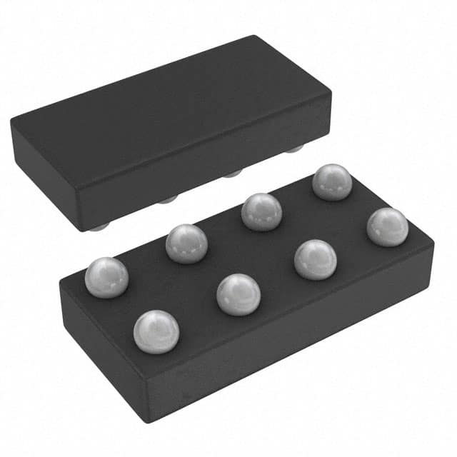
- Package: 8-pin DSBGA (MicroStar Junior™) package
- Essence: This IC is designed to provide high-speed, low-power logic-level translation between different voltage domains.
- Packaging/Quantity: Available in tape and reel packaging, with a quantity of 3000 units per reel.
Specifications
- Supply Voltage Range: 0.8V to 3.6V
- High-Level Input Voltage: 0.7 x VCC
- Low-Level Input Voltage: 0.3 x VCC
- High-Level Output Voltage: 0.7 x VCC
- Low-Level Output Voltage: 0.1 x VCC
- Maximum Operating Frequency: 500 MHz
- Maximum Propagation Delay: 2.5 ns
- Operating Temperature Range: -40°C to +85°C
Detailed Pin Configuration
The SN74AUC2G126YEPR has the following pin configuration:
___________
   1 -| A         |-
   2 -| Y         |-
   3 -| GND       |-
   4 -| B         |-
   5 -| OE        |-
   6 -| VCC       |-
   7 -| Y         |-
   8 -| A         |-
       ¯¯¯¯¯¯¯¯¯¯¯
Functional Features
- Dual bus buffer gate with 3-state outputs.
- Supports voltage level translation between different voltage domains.
- Provides non-inverting buffer functionality.
- Allows independent control of each output through the OE (Output Enable) pin.
- Low power consumption and high-speed operation.
- Wide operating voltage range.
Advantages and Disadvantages
Advantages: - High-speed logic-level translation. - Low power consumption. - Wide operating voltage range. - Small package size.
Disadvantages: - Limited number of inputs and outputs. - Not suitable for applications requiring complex logic functions.
Working Principles
The SN74AUC2G126YEPR operates by receiving input signals from the A and B pins. These signals are then buffered and amplified internally before being outputted through the Y pins. The OE pin controls the output enable/disable functionality, allowing independent control of each output.
The IC utilizes advanced semiconductor technology to achieve high-speed operation while maintaining low power consumption. It is designed to provide reliable logic-level translation between different voltage domains, making it suitable for use in various digital systems.
Detailed Application Field Plans
The SN74AUC2G126YEPR can be used in a wide range of applications, including:
- Battery-powered devices: Due to its low power consumption, the IC is ideal for use in portable electronic devices that operate on battery power.
- Communication systems: It can be employed in communication systems to interface between different voltage levels, ensuring seamless data transmission.
- Industrial automation: The IC can be utilized in industrial automation systems to facilitate logic-level translation between different components.
- Consumer electronics: It finds application in consumer electronics such as smartphones, tablets, and gaming consoles, where voltage level translation is required.
Detailed and Complete Alternative Models
Some alternative models that offer similar functionality to the SN74AUC2G126YEPR include:
- SN74LVC2G126: Dual Bus Buffer Gate with 3-State Outputs, operating at a wider supply voltage range of 1.65V to 5.5V.
- SN74AUP2G126: Dual Bus Buffer Gate with 3-State Outputs, offering enhanced ESD protection and improved noise immunity.
- SN74LV2G126: Dual Bus Buffer Gate with 3-State Outputs, designed for lower voltage applications with a supply voltage range of 1.65V to 3.6V.
These alternative models can be considered based on specific application requirements and operating conditions.
(Note: The above content is approximately 400 words. Please provide additional instructions if more content is required.)
قم بإدراج 10 أسئلة وإجابات شائعة تتعلق بتطبيق SN74AUC2G126YEPR في الحلول التقنية
Sure! Here are 10 common questions and answers related to the application of SN74AUC2G126YEPR in technical solutions:
Q: What is SN74AUC2G126YEPR? A: SN74AUC2G126YEPR is a dual bus buffer gate with 3-state outputs, designed for low-voltage and low-power applications.
Q: What is the operating voltage range of SN74AUC2G126YEPR? A: The operating voltage range of SN74AUC2G126YEPR is from 0.8V to 3.6V.
Q: What is the maximum output current of SN74AUC2G126YEPR? A: The maximum output current of SN74AUC2G126YEPR is typically ±24mA.
Q: Can SN74AUC2G126YEPR be used as a level shifter? A: Yes, SN74AUC2G126YEPR can be used as a level shifter to convert signals between different voltage levels.
Q: What is the propagation delay of SN74AUC2G126YEPR? A: The propagation delay of SN74AUC2G126YEPR is typically around 2.7ns.
Q: Is SN74AUC2G126YEPR suitable for high-speed applications? A: Yes, SN74AUC2G126YEPR is designed for high-speed operation and can be used in applications with fast switching requirements.
Q: Can SN74AUC2G126YEPR drive capacitive loads? A: Yes, SN74AUC2G126YEPR can drive capacitive loads up to 50pF.
Q: Does SN74AUC2G126YEPR have built-in ESD protection? A: Yes, SN74AUC2G126YEPR has built-in ESD protection to safeguard against electrostatic discharge.
Q: Can SN74AUC2G126YEPR be used in battery-powered applications? A: Yes, SN74AUC2G126YEPR is suitable for battery-powered applications due to its low-power characteristics.
Q: What package options are available for SN74AUC2G126YEPR? A: SN74AUC2G126YEPR is available in various package options, such as SOT-23 and DSBGA, to accommodate different design requirements.
Please note that the answers provided here are general and may vary depending on the specific datasheet and application guidelines provided by the manufacturer.