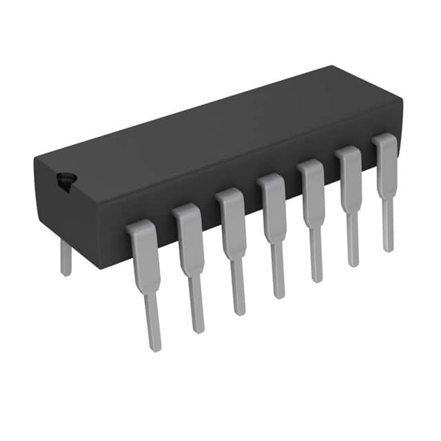
SN74LS09NG4
Product Overview
Category
SN74LS09NG4 belongs to the category of integrated circuits (ICs).
Use
This product is commonly used in digital logic circuits for performing logical AND operations.
Characteristics
- Low power consumption
- High-speed operation
- Wide operating voltage range
- TTL compatible inputs and outputs
Package
SN74LS09NG4 is available in a 14-pin DIP (Dual In-line Package) format.
Essence
The essence of SN74LS09NG4 lies in its ability to perform logical AND operations efficiently and reliably.
Packaging/Quantity
SN74LS09NG4 is typically packaged in reels or tubes, with each reel or tube containing a specific quantity of ICs. The exact packaging and quantity may vary depending on the manufacturer.
Specifications
- Supply Voltage: 4.75V to 5.25V
- Operating Temperature Range: -40°C to +85°C
- Input Voltage: 2V (maximum)
- Output Voltage: 0.4V (maximum)
- Propagation Delay Time: 9ns (typical)
Detailed Pin Configuration
SN74LS09NG4 has a total of 14 pins, which are labeled as follows:
- A1 (Input A1)
- B1 (Input B1)
- Y1 (Output Y1)
- A2 (Input A2)
- B2 (Input B2)
- Y2 (Output Y2)
- GND (Ground)
- Y3 (Output Y3)
- B3 (Input B3)
- A3 (Input A3)
- Y4 (Output Y4)
- B4 (Input B4)
- A4 (Input A4)
- VCC (Supply Voltage)
Functional Features
SN74LS09NG4 is a quad 2-input AND gate. It consists of four independent AND gates, each with two inputs and one output. The inputs are TTL compatible, allowing easy integration into existing digital logic circuits. The outputs are also TTL compatible, ensuring compatibility with other devices in the circuit.
Advantages and Disadvantages
Advantages
- Low power consumption makes it suitable for battery-powered applications.
- High-speed operation enables efficient processing of logical AND operations.
- Wide operating voltage range allows flexibility in different power supply configurations.
- TTL compatibility simplifies integration into existing digital logic circuits.
Disadvantages
- Limited number of inputs (two per gate) may restrict complex logic operations.
- Propagation delay time may impact the overall performance in high-speed applications.
Working Principles
SN74LS09NG4 operates based on the principles of Boolean logic. Each of the four independent AND gates within the IC performs a logical AND operation on its respective inputs and produces an output based on the input combination. The outputs reflect the result of the logical AND operation performed by each gate.
Detailed Application Field Plans
SN74LS09NG4 finds applications in various fields where logical AND operations are required. Some common application areas include: - Digital signal processing - Microprocessor-based systems - Communication systems - Industrial automation - Robotics
Detailed and Complete Alternative Models
There are several alternative models available that serve similar functions to SN74LS09NG4. Some notable alternatives include: - 74HC08: Quad 2-input AND gate with CMOS technology - CD4081: Quad 2-input AND gate with CMOS technology - MC14008: Quad 2-input AND gate with MOS technology
These alternative models offer similar functionality but may differ in terms of specific characteristics, package types, or voltage ranges. It is important to consider the requirements of the specific application when selecting an alternative model.
In conclusion, SN74LS09NG4 is a versatile integrated circuit that provides efficient logical AND operations. Its low power consumption, high-speed operation, and wide operating voltage range make it suitable for various digital logic applications. However, its limited number of inputs and propagation delay time should be considered in certain scenarios.
قم بإدراج 10 أسئلة وإجابات شائعة تتعلق بتطبيق SN74LS09NG4 في الحلول التقنية
Sure! Here are 10 common questions and answers related to the application of SN74LS09NG4 in technical solutions:
Q: What is SN74LS09NG4? A: SN74LS09NG4 is a quad 2-input AND gate integrated circuit (IC) that is commonly used in digital logic circuits.
Q: What is the purpose of SN74LS09NG4? A: The purpose of SN74LS09NG4 is to perform logical AND operations on two input signals, producing an output signal based on their logical states.
Q: What voltage levels does SN74LS09NG4 support? A: SN74LS09NG4 supports TTL (Transistor-Transistor Logic) voltage levels, typically operating at 5V.
Q: How many AND gates are there in SN74LS09NG4? A: SN74LS09NG4 contains four independent AND gates, each with two inputs and one output.
Q: Can SN74LS09NG4 be used for both positive and negative logic applications? A: Yes, SN74LS09NG4 can be used for both positive and negative logic applications, depending on how the inputs and outputs are connected.
Q: What is the maximum frequency at which SN74LS09NG4 can operate? A: SN74LS09NG4 can typically operate at frequencies up to 25 MHz.
Q: Can SN74LS09NG4 drive other ICs directly? A: No, SN74LS09NG4 has limited output current capabilities and may require additional buffering to drive other ICs directly.
Q: Is SN74LS09NG4 suitable for high-speed applications? A: While SN74LS09NG4 can operate at moderate frequencies, it may not be the best choice for high-speed applications due to its propagation delay.
Q: Can SN74LS09NG4 be used in both digital and analog circuits? A: No, SN74LS09NG4 is specifically designed for digital logic applications and is not suitable for use in analog circuits.
Q: Are there any special considerations when using SN74LS09NG4 in noisy environments? A: Yes, SN74LS09NG4 is susceptible to noise interference, so proper decoupling and grounding techniques should be employed to minimize noise-related issues.
Please note that these answers are general and may vary depending on specific application requirements.


