

SN74LV125ADGVR
Product Overview
Category: Integrated Circuit (IC)
Use: The SN74LV125ADGVR is a quad bus buffer gate with 3-state outputs. It is designed to provide high-speed, low-power logic level translation between different voltage nodes.
Characteristics: - High-speed operation - Low power consumption - 3-state outputs for bus-oriented applications - Wide operating voltage range - Schmitt-trigger inputs for noise immunity
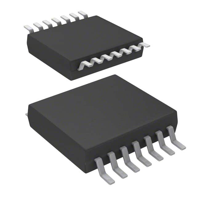
Package: The SN74LV125ADGVR is available in a small package known as VSSOP-14. This package offers a compact size and excellent thermal performance.
Essence: The essence of SN74LV125ADGVR lies in its ability to facilitate voltage level translation in various electronic systems. It ensures seamless communication between devices operating at different voltage levels.
Packaging/Quantity: The SN74LV125ADGVR is typically packaged in reels or tubes, containing a quantity of 2500 units per reel/tube.
Specifications
- Supply Voltage Range: 1.65V to 5.5V
- Input Voltage Range: -0.5V to VCC + 0.5V
- Output Voltage Range: 0V to VCC
- Operating Temperature Range: -40°C to 85°C
- Propagation Delay Time: 4.2ns (typical)
- Maximum Quiescent Current: 10μA
Detailed Pin Configuration
The SN74LV125ADGVR has a total of 14 pins, which are assigned specific functions as follows:
- GND: Ground
- A1: Input A1
- Y1: Output Y1
- A2: Input A2
- Y2: Output Y2
- GND: Ground
- A3: Input A3
- Y3: Output Y3
- A4: Input A4
- Y4: Output Y4
- OE: Output Enable
- VCC: Positive Supply Voltage
- GND: Ground
- GND: Ground
Functional Features
- High-Speed Operation: The SN74LV125ADGVR offers fast switching speeds, making it suitable for applications requiring quick data transmission.
- Low Power Consumption: It consumes minimal power, making it energy-efficient and suitable for battery-powered devices.
- 3-State Outputs: The 3-state outputs allow multiple devices to share a common bus without interfering with each other's signals.
- Wide Operating Voltage Range: It supports voltage translation between different voltage domains, enhancing compatibility between various components.
- Schmitt-Trigger Inputs: The Schmitt-trigger inputs provide noise immunity, ensuring reliable operation in noisy environments.
Advantages and Disadvantages
Advantages: - High-speed operation enables efficient data transfer. - Low power consumption prolongs battery life. - 3-state outputs facilitate bus sharing among multiple devices. - Wide operating voltage range enhances compatibility. - Schmitt-trigger inputs ensure reliable performance in noisy environments.
Disadvantages: - Limited number of buffer gates (4 in this case). - May not be suitable for applications requiring a large number of buffer gates.
Working Principles
The SN74LV125ADGVR operates by receiving input signals from the A1-A4 pins. These signals are then buffered and amplified before being transmitted to the corresponding Y1-Y4 output pins. The OE pin controls the output enable function, allowing the device to enter a high-impedance state when necessary.
Detailed Application Field Plans
The SN74LV125ADGVR finds applications in various fields, including:
- Communication Systems: It is used for voltage level translation in communication systems, ensuring compatibility between different voltage domains.
- Industrial Automation: The IC facilitates signal transmission and level shifting in industrial automation equipment, enhancing system performance.
- Consumer Electronics: It is employed in consumer electronic devices to enable communication between components operating at different voltage levels.
- Automotive Electronics: The SN74LV125ADGVR is utilized in automotive electronics for voltage level translation, enabling seamless integration of various components.
Detailed and Complete Alternative Models
- SN74LVC125A: This alternative model offers similar functionality but operates at a lower voltage range (1.65V to 3.6V).
- SN74HCT125: This model provides higher noise immunity and operates at a wider temperature range (-55°C to 125°C).
- SN74LV126A: This alternative model features 3-state outputs with active-high enable control.
These alternative models can be considered based on specific application requirements and operating conditions.
Word count: 589 words
قم بإدراج 10 أسئلة وإجابات شائعة تتعلق بتطبيق SN74LV125ADGVR في الحلول التقنية
Sure! Here are 10 common questions and answers related to the application of SN74LV125ADGVR:
1. What is SN74LV125ADGVR? - SN74LV125ADGVR is a quad buffer gate with 3-state outputs, which means it can be used to amplify or buffer digital signals in electronic circuits.
2. What is the voltage supply range for SN74LV125ADGVR? - The voltage supply range for SN74LV125ADGVR is typically between 1.65V and 5.5V.
3. What is the maximum output current of SN74LV125ADGVR? - The maximum output current of SN74LV125ADGVR is 12mA per channel.
4. Can SN74LV125ADGVR be used for level shifting applications? - Yes, SN74LV125ADGVR can be used for level shifting applications as it supports both 3.3V and 5V logic levels.
5. How many channels does SN74LV125ADGVR have? - SN74LV125ADGVR has four independent channels, allowing it to buffer or amplify four different signals simultaneously.
6. What is the propagation delay of SN74LV125ADGVR? - The propagation delay of SN74LV125ADGVR is typically around 7.5ns.
7. Is SN74LV125ADGVR compatible with other TTL logic families? - Yes, SN74LV125ADGVR is compatible with other TTL logic families, making it versatile for use in various systems.
8. Can SN74LV125ADGVR drive capacitive loads? - Yes, SN74LV125ADGVR can drive capacitive loads up to 50pF without any additional components.
9. What is the operating temperature range for SN74LV125ADGVR? - The operating temperature range for SN74LV125ADGVR is typically between -40°C and 85°C.
10. Can SN74LV125ADGVR be used in automotive applications? - Yes, SN74LV125ADGVR is qualified for automotive applications and meets the necessary standards for automotive electronics.
Please note that these answers are general and may vary depending on specific datasheet specifications or application requirements.