

SN74LV125AQRGYRQ1
Product Overview
Category
SN74LV125AQRGYRQ1 belongs to the category of integrated circuits (ICs).
Use
This IC is commonly used as a quad bus buffer gate with 3-state outputs.
Characteristics
- Low-voltage operation: This IC operates at low voltage levels, making it suitable for use in low-power applications.
- High-speed performance: SN74LV125AQRGYRQ1 offers high-speed operation, enabling efficient data transmission.
- 3-state outputs: The IC features 3-state outputs, allowing multiple devices to share a common bus without interference.
- Wide operating temperature range: It can operate reliably across a wide temperature range, making it suitable for various environments.
Package
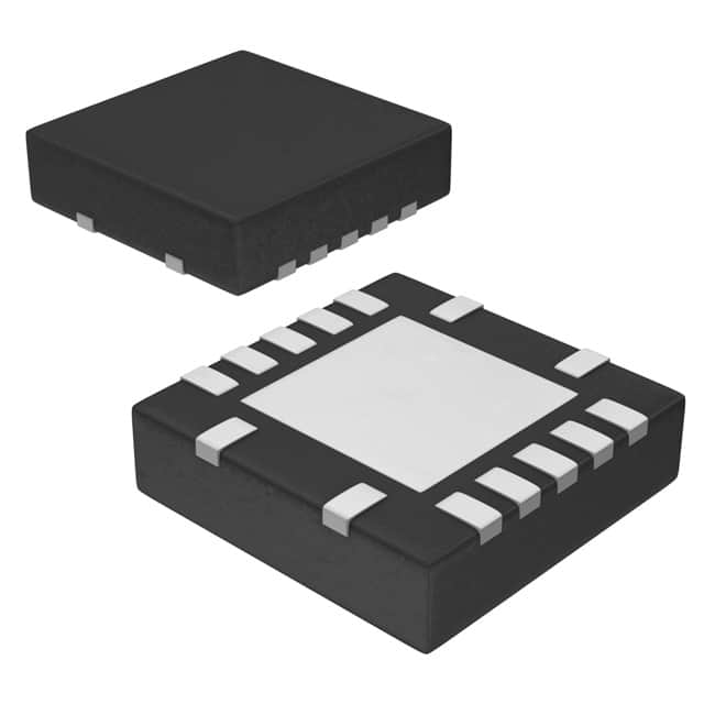
SN74LV125AQRGYRQ1 is available in a small-outline package (SOIC) with 14 pins.
Essence
The essence of SN74LV125AQRGYRQ1 lies in its ability to buffer and control the flow of data signals in electronic circuits.
Packaging/Quantity
This IC is typically packaged in reels or tubes, with a quantity of 2500 units per reel/tube.
Specifications
- Supply Voltage Range: 2 V to 5.5 V
- Input Voltage Range: 0 V to VCC
- Output Voltage Range: 0 V to VCC
- Operating Temperature Range: -40°C to +125°C
- Maximum Operating Frequency: 100 MHz
- Output Current: ±8 mA
Detailed Pin Configuration
The pin configuration of SN74LV125AQRGYRQ1 is as follows:
```
| | --|1 14 |-- VCC --|2 13 |-- A1 --|3 12 |-- Y1 --|4 11 |-- A2 --|5 10 |-- Y2 --|6 9 |-- GND --|7 8 |-- G1 |___________| ```
Functional Features
- Quad buffer gate: SN74LV125AQRGYRQ1 consists of four independent buffer gates, allowing for simultaneous operation on multiple data lines.
- 3-state outputs: The IC offers 3-state outputs, enabling the control of data flow and preventing bus contention.
- High-speed operation: With a maximum operating frequency of 100 MHz, this IC ensures efficient data transmission.
Advantages and Disadvantages
Advantages
- Low-voltage operation makes it suitable for low-power applications.
- Wide operating temperature range allows for reliable performance in various environments.
- 3-state outputs enable multiple devices to share a common bus without interference.
Disadvantages
- Limited output current may restrict its use in certain high-current applications.
- Availability in only one package type (SOIC) may limit compatibility with specific circuit designs.
Working Principles
SN74LV125AQRGYRQ1 operates by receiving input signals and buffering them to the corresponding output pins. The 3-state outputs allow the IC to control the flow of data on the bus, ensuring proper communication between multiple devices.
Detailed Application Field Plans
SN74LV125AQRGYRQ1 finds application in various fields, including: - Microcontrollers and microprocessors - Communication systems - Industrial automation - Automotive electronics - Consumer electronics
Detailed and Complete Alternative Models
Some alternative models that can be considered as alternatives to SN74LV125AQRGYRQ1 are: - SN74LVC125A: Similar functionality with improved voltage tolerance. - SN74HC125: Higher speed operation but requires higher supply voltage. - SN74LV126A: Similar functionality with additional output enable feature.
These alternative models offer similar or enhanced features, providing flexibility in choosing the most suitable IC for specific applications.
Word count: 511 words
قم بإدراج 10 أسئلة وإجابات شائعة تتعلق بتطبيق SN74LV125AQRGYRQ1 في الحلول التقنية
Sure! Here are 10 common questions and answers related to the application of SN74LV125AQRGYRQ1 in technical solutions:
1. What is SN74LV125AQRGYRQ1? - SN74LV125AQRGYRQ1 is a quad bus buffer gate with 3-state outputs, designed for voltage translation applications.
2. What is the operating voltage range of SN74LV125AQRGYRQ1? - The operating voltage range is from 1.65V to 5.5V.
3. How many channels does SN74LV125AQRGYRQ1 have? - SN74LV125AQRGYRQ1 has four independent channels.
4. What is the maximum output current of SN74LV125AQRGYRQ1? - The maximum output current per channel is ±12mA.
5. Can SN74LV125AQRGYRQ1 be used for level shifting? - Yes, SN74LV125AQRGYRQ1 can be used for level shifting between different voltage domains.
6. What is the propagation delay of SN74LV125AQRGYRQ1? - The typical propagation delay is 4.8ns.
7. Is SN74LV125AQRGYRQ1 suitable for high-speed applications? - Yes, SN74LV125AQRGYRQ1 is designed for high-speed operation and can be used in various high-frequency applications.
8. Does SN74LV125AQRGYRQ1 have internal pull-up or pull-down resistors? - No, SN74LV125AQRGYRQ1 does not have internal pull-up or pull-down resistors.
9. Can SN74LV125AQRGYRQ1 be used in automotive applications? - Yes, SN74LV125AQRGYRQ1 is qualified for automotive applications and meets the AEC-Q100 standard.
10. What is the package type of SN74LV125AQRGYRQ1? - SN74LV125AQRGYRQ1 is available in a 14-pin VQFN package.
Please note that these answers are general and may vary depending on the specific requirements and use cases. It's always recommended to refer to the datasheet and consult with the manufacturer for detailed information.