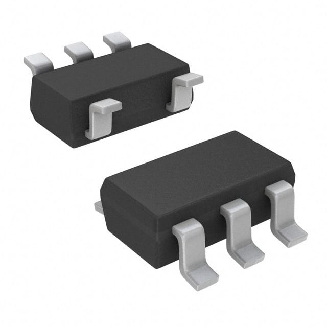
SN74LVC1G00DCKJ
Overview
- Category: Integrated Circuit (IC)
- Use: Logic Gate
- Characteristics: Single 2-Input NAND Gate
- Package: SC-70 (6-Pin SOT-363)
- Essence: High-Speed CMOS Logic
- Packaging/Quantity: Tape and Reel, 3000 pieces per reel
Specifications
- Supply Voltage Range: 1.65V to 5.5V
- Input Voltage Range: -0.5V to VCC + 0.5V
- Output Voltage Range: 0V to VCC
- Maximum Operating Frequency: 100 MHz
- Propagation Delay: 3.8 ns (typical)
- Low Power Consumption: ICC = 1 µA (maximum)
Detailed Pin Configuration
The SN74LVC1G00DCKJ has the following pin configuration:
____
   A --|    |-- VCC
   B --|    |-- Y
 GND --|____|-- NC
Functional Features
- High-Speed Operation: The SN74LVC1G00DCKJ is designed for high-speed logic applications, allowing for fast signal processing.
- Wide Voltage Range: It can operate within a wide supply voltage range of 1.65V to 5.5V, making it compatible with various systems.
- Low Power Consumption: With a maximum current consumption of only 1 µA, it helps conserve power in battery-operated devices.
- Schmitt-Trigger Inputs: The inputs have Schmitt-trigger characteristics, providing hysteresis and improving noise immunity.
Advantages and Disadvantages
Advantages: - Small Package Size: The SC-70 package allows for compact circuit designs, especially in space-constrained applications. - High-Speed Operation: The SN74LVC1G00DCKJ offers fast propagation delay, enabling efficient signal processing. - Wide Voltage Range: It can be used in a wide range of systems with different supply voltages.
Disadvantages: - Single Gate: The IC only contains a single 2-input NAND gate, limiting its functionality compared to multi-gate ICs. - Limited Output Current: The output current is limited to a maximum of 32 mA, which may not be sufficient for certain applications.
Working Principles
The SN74LVC1G00DCKJ operates based on complementary metal-oxide-semiconductor (CMOS) technology. It utilizes MOSFET transistors to implement the logic function of a 2-input NAND gate. When both input A and input B are high, the output Y becomes low. In all other cases, the output remains high.
Detailed Application Field Plans
The SN74LVC1G00DCKJ can be used in various applications, including but not limited to:
- Digital Logic Circuits: It can be employed as a basic building block for constructing more complex digital logic circuits.
- Signal Processing: The high-speed operation makes it suitable for signal processing tasks, such as waveform generation and data manipulation.
- Microcontrollers and Microprocessors: It can be utilized in microcontroller and microprocessor-based systems for general-purpose logic operations.
- Communication Systems: The IC can be integrated into communication systems to perform logical functions in data transmission and reception.
Detailed and Complete Alternative Models
- SN74LVC1G00DBVR: SOT-23 package, 3000 pieces per reel
- SN74LVC1G00DRLR: X2SON package, 2500 pieces per reel
- SN74LVC1G00YZPR: DSBGA package, 4000 pieces per reel
- SN74LVC1G00DCKR: SC-70 package, 3000 pieces per reel
These alternative models offer similar functionality and characteristics to the SN74LVC1G00DCKJ, providing flexibility in choosing the most suitable option for specific applications.
Word count: 442 words
قم بإدراج 10 أسئلة وإجابات شائعة تتعلق بتطبيق SN74LVC1G00DCKJ في الحلول التقنية
Sure! Here are 10 common questions and answers related to the application of SN74LVC1G00DCKJ:
Q1: What is SN74LVC1G00DCKJ? A1: SN74LVC1G00DCKJ is a single 2-input NAND gate integrated circuit (IC) from Texas Instruments.
Q2: What is the voltage range supported by SN74LVC1G00DCKJ? A2: SN74LVC1G00DCKJ supports a voltage range of 1.65V to 5.5V.
Q3: What is the maximum output current of SN74LVC1G00DCKJ? A3: The maximum output current of SN74LVC1G00DCKJ is 32mA.
Q4: Can SN74LVC1G00DCKJ be used in battery-powered applications? A4: Yes, SN74LVC1G00DCKJ can be used in battery-powered applications due to its low power consumption.
Q5: What is the typical propagation delay of SN74LVC1G00DCKJ? A5: The typical propagation delay of SN74LVC1G00DCKJ is around 4.3ns.
Q6: Is SN74LVC1G00DCKJ compatible with other logic families? A6: Yes, SN74LVC1G00DCKJ is compatible with both CMOS and TTL logic families.
Q7: Can SN74LVC1G00DCKJ drive capacitive loads? A7: Yes, SN74LVC1G00DCKJ can drive capacitive loads up to 50pF.
Q8: What is the operating temperature range of SN74LVC1G00DCKJ? A8: SN74LVC1G00DCKJ has an operating temperature range of -40°C to 125°C.
Q9: Can SN74LVC1G00DCKJ be used in high-speed applications? A9: Yes, SN74LVC1G00DCKJ can be used in high-speed applications due to its low propagation delay.
Q10: What is the package type of SN74LVC1G00DCKJ? A10: SN74LVC1G00DCKJ comes in a small SOT-353 package.


