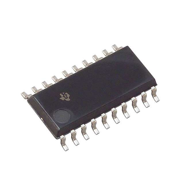
SN74LVC245ANSRG4
Product Overview
Category
SN74LVC245ANSRG4 belongs to the category of integrated circuits (ICs).
Use
This IC is commonly used for level shifting and voltage translation applications.
Characteristics
- Low-voltage CMOS technology
- Bidirectional voltage-level translation
- Supports voltages from 1.65V to 5.5V
- High-speed operation
- 8-bit wide data bus
- Non-inverting outputs
- Schmitt-trigger inputs
- ESD protection on all inputs and outputs
Package
SN74LVC245ANSRG4 is available in a small-outline, no-lead (SON) package.
Essence
The essence of SN74LVC245ANSRG4 lies in its ability to provide bidirectional voltage-level translation between different voltage domains.
Packaging/Quantity
This IC is typically packaged in reels and comes in quantities of 2500 units per reel.
Specifications
- Supply Voltage Range: 1.65V to 5.5V
- Input Voltage Range: 0V to VCC
- Output Voltage Range: 0V to VCC
- Operating Temperature Range: -40°C to +85°C
- Propagation Delay: 3.6ns (max)
- Output Drive Capability: ±24mA
- ESD Protection: Human Body Model (HBM) > 2000V
Detailed Pin Configuration
The SN74LVC245ANSRG4 IC has a total of 20 pins. The pin configuration is as follows:
- DIR (Direction Control)
- OE (Output Enable)
- A1 (Input/Output)
- B1 (Input/Output)
- A2 (Input/Output)
- B2 (Input/Output)
- A3 (Input/Output)
- B3 (Input/Output)
- A4 (Input/Output)
- B4 (Input/Output)
- GND (Ground)
- B5 (Input/Output)
- A5 (Input/Output)
- B6 (Input/Output)
- A6 (Input/Output)
- B7 (Input/Output)
- A7 (Input/Output)
- B8 (Input/Output)
- A8 (Input/Output)
- VCC (Supply Voltage)
Functional Features
- Bidirectional voltage-level translation between different voltage domains
- Non-inverting outputs for direct compatibility with various logic families
- Schmitt-trigger inputs for improved noise immunity
- ESD protection on all inputs and outputs for enhanced reliability
- High-speed operation for efficient data transfer
Advantages and Disadvantages
Advantages
- Wide supply voltage range allows compatibility with a variety of systems
- Bidirectional functionality simplifies circuit design
- High-speed operation enables fast data transfer
- ESD protection ensures robustness against electrostatic discharge
Disadvantages
- Limited number of input/output pins (8-bit wide data bus)
- May require additional external components for specific applications
Working Principles
SN74LVC245ANSRG4 operates by receiving input signals from one voltage domain and translating them to the corresponding voltage level in another domain. The direction of translation is controlled by the DIR pin. When DIR is set to high, the IC translates signals from A1-A8 to B1-B8. Conversely, when DIR is low, the translation occurs in the opposite direction.
Detailed Application Field Plans
SN74LVC245ANSRG4 finds applications in various fields, including:
- Microcontroller interfacing
- Level shifting in mixed-voltage systems
- Communication interfaces (e.g., UART, SPI, I2C)
- Sensor interfacing
- Data acquisition systems
Detailed and Complete Alternative Models
- SN74LVC245APW - TSSOP package, 20 pins
- SN74LVC245ADGVR - TVSOP package, 20 pins
- SN74LVC245ARGYR - VQFN package, 20 pins
- SN74LVC245ANSR - SOP package, 20 pins
- SN74LVC245APWRG4 - TSSOP package, 20 pins
These alternative models offer similar functionality to SN74LVC245ANSRG4 but may differ in package type or pin configuration.
Word count: 536 words
قم بإدراج 10 أسئلة وإجابات شائعة تتعلق بتطبيق SN74LVC245ANSRG4 في الحلول التقنية
Sure! Here are 10 common questions and answers related to the application of SN74LVC245ANSRG4:
Q: What is the SN74LVC245ANSRG4? A: The SN74LVC245ANSRG4 is a high-performance octal bus transceiver with 3-state outputs. It can be used for level shifting and voltage translation in various digital applications.
Q: What is the operating voltage range of SN74LVC245ANSRG4? A: The operating voltage range of SN74LVC245ANSRG4 is from 1.65V to 5.5V.
Q: How many bidirectional channels does SN74LVC245ANSRG4 have? A: SN74LVC245ANSRG4 has 8 bidirectional channels, allowing data transmission in both directions.
Q: What is the maximum data transfer rate supported by SN74LVC245ANSRG4? A: SN74LVC245ANSRG4 supports a maximum data transfer rate of 100Mbps.
Q: Can SN74LVC245ANSRG4 handle mixed-voltage systems? A: Yes, SN74LVC245ANSRG4 is designed to handle mixed-voltage systems, making it suitable for interfacing between different logic families.
Q: Does SN74LVC245ANSRG4 have built-in ESD protection? A: Yes, SN74LVC245ANSRG4 has built-in ESD protection, ensuring robustness against electrostatic discharge events.
Q: What is the output drive strength of SN74LVC245ANSRG4? A: SN74LVC245ANSRG4 has a typical output drive strength of ±24mA, allowing it to drive capacitive loads and long traces.
Q: Can SN74LVC245ANSRG4 be used in automotive applications? A: Yes, SN74LVC245ANSRG4 is qualified for automotive applications and meets the necessary standards.
Q: Does SN74LVC245ANSRG4 support hot insertion? A: Yes, SN74LVC245ANSRG4 supports hot insertion, allowing it to be plugged or unplugged while the power is still applied.
Q: What package options are available for SN74LVC245ANSRG4? A: SN74LVC245ANSRG4 is available in various package options, including SOIC, TSSOP, and VQFN, providing flexibility for different PCB layouts and space constraints.
Please note that these answers are general and may vary depending on the specific datasheet and application requirements.


