

SN74LVC2G17DRYR
Product Overview
- Category: Integrated Circuit (IC)
- Use: Logic Gate
- Characteristics: Dual Schmitt-Trigger Buffer/Driver
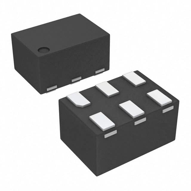
- Package: VSSOP (Very Small Outline Package)
- Essence: This IC is designed to provide buffering and driving capabilities for digital signals in various electronic circuits.
- Packaging/Quantity: Available in reels, with a quantity of 3000 units per reel.
Specifications
- Supply Voltage Range: 1.65V to 5.5V
- Input Voltage Range: -0.5V to 7V
- Output Voltage Range: 0V to VCC
- Operating Temperature Range: -40°C to +85°C
- Propagation Delay: 3.8ns (typical)
- Output Drive Capability: ±24mA
Detailed Pin Configuration
The SN74LVC2G17DRYR has a total of 6 pins:
- Pin 1: Input A
- Pin 2: Output Y
- Pin 3: Ground (GND)
- Pin 4: Power Supply (VCC)
- Pin 5: Input B
- Pin 6: Output Y
Functional Features
- Dual Schmitt-trigger buffer/driver with open-drain outputs
- Provides signal buffering and driving capabilities
- Schmitt-trigger inputs allow for hysteresis and noise immunity
- Low power consumption
- High-speed operation
- Supports wide supply voltage range
Advantages and Disadvantages
Advantages: - Dual functionality allows for versatile use in different circuit designs - Open-drain outputs enable easy interfacing with other components - Hysteresis and noise immunity provided by Schmitt-trigger inputs enhance signal integrity - Wide supply voltage range allows for compatibility with various power sources
Disadvantages: - Limited output drive capability may not be suitable for high-current applications - Propagation delay of 3.8ns may introduce timing issues in certain circuits
Working Principles
The SN74LVC2G17DRYR operates as a dual Schmitt-trigger buffer/driver. It receives digital input signals from pins A and B, and based on the input voltage levels, it provides corresponding buffered outputs on pins Y. The Schmitt-trigger inputs ensure that the output transitions occur at different voltage thresholds for rising and falling edges, providing hysteresis and noise immunity.
Detailed Application Field Plans
The SN74LVC2G17DRYR finds application in various electronic circuits where buffering and driving of digital signals are required. Some common application fields include:
- Communication Systems: Used for signal conditioning and level shifting in communication interfaces.
- Industrial Automation: Employed in control systems to interface between microcontrollers and actuators/sensors.
- Automotive Electronics: Integrated into automotive modules for signal amplification and level conversion.
- Consumer Electronics: Utilized in devices like smartphones, tablets, and gaming consoles for signal processing and interfacing.
Detailed and Complete Alternative Models
- SN74LVC2G17DCKR: Similar functionality but available in SC-70 package.
- SN74LVC2G17DBVR: Similar functionality but available in SOT-23 package.
- SN74LVC2G17DCUR: Similar functionality but available in USON package.
These alternative models provide similar features and performance characteristics, allowing users to choose the most suitable option based on their specific requirements.
Word count: 431 words
قم بإدراج 10 أسئلة وإجابات شائعة تتعلق بتطبيق SN74LVC2G17DRYR في الحلول التقنية
Sure! Here are 10 common questions and answers related to the application of SN74LVC2G17DRYR in technical solutions:
Q: What is SN74LVC2G17DRYR? A: SN74LVC2G17DRYR is a dual Schmitt-trigger buffer/driver integrated circuit (IC) that can be used for signal conditioning and level shifting applications.
Q: What is the operating voltage range of SN74LVC2G17DRYR? A: SN74LVC2G17DRYR operates within a voltage range of 1.65V to 5.5V.
Q: What is the maximum output current of SN74LVC2G17DRYR? A: The maximum output current of SN74LVC2G17DRYR is typically 32mA.
Q: Can SN74LVC2G17DRYR be used as a level shifter? A: Yes, SN74LVC2G17DRYR can be used as a level shifter to convert signals between different voltage levels.
Q: What is the input hysteresis of SN74LVC2G17DRYR? A: SN74LVC2G17DRYR has an input hysteresis of typically 0.5V, which helps improve noise immunity.
Q: Is SN74LVC2G17DRYR suitable for high-speed applications? A: Yes, SN74LVC2G17DRYR is designed for high-speed operation and can support data rates up to several hundred megahertz.
Q: Can SN74LVC2G17DRYR drive capacitive loads? A: Yes, SN74LVC2G17DRYR can drive capacitive loads up to 50pF.
Q: Does SN74LVC2G17DRYR have built-in ESD protection? A: Yes, SN74LVC2G17DRYR has built-in ESD protection, which helps safeguard against electrostatic discharge events.
Q: What is the package type of SN74LVC2G17DRYR? A: SN74LVC2G17DRYR is available in a small SOT-23-6 package.
Q: Can SN74LVC2G17DRYR be used in battery-powered applications? A: Yes, SN74LVC2G17DRYR's low power consumption and wide operating voltage range make it suitable for battery-powered applications.
Please note that these answers are general and may vary depending on specific application requirements and datasheet specifications.