

SN74LVC3G34YZAR
Product Overview
- Category: Integrated Circuit (IC)
- Use: Logic Gate
- Characteristics: Triple Buffer/Inverter with Open-Drain Outputs
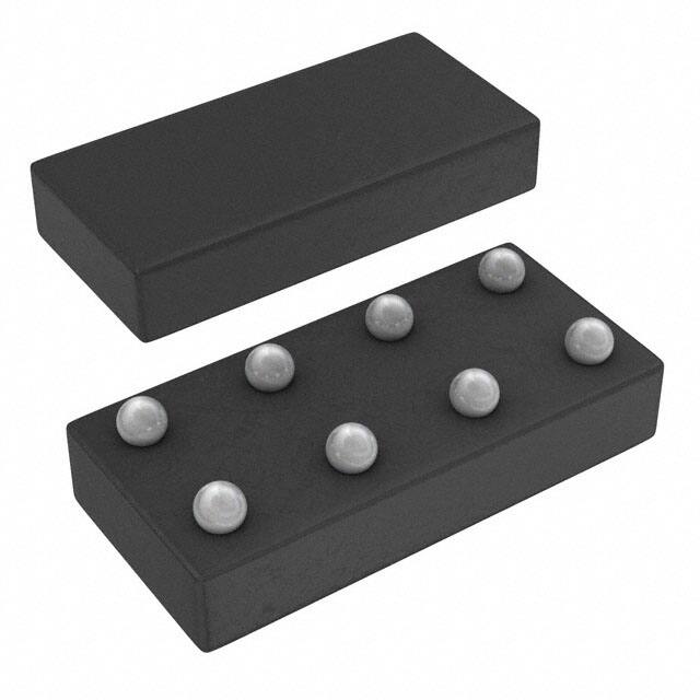
- Package: 8-Bump micro SMD (YZA) package
- Essence: High-speed CMOS technology for low power consumption and high noise immunity
- Packaging/Quantity: Tape and Reel, 3000 units per reel
Specifications
- Supply Voltage Range: 1.65V to 5.5V
- Input Voltage Range: -0.5V to VCC + 0.5V
- Output Voltage Range: -0.5V to VCC + 0.5V
- Maximum Operating Frequency: 100 MHz
- Propagation Delay: 2.4 ns (typical)
- Low Power Consumption: ICC = 1 µA (maximum)
Detailed Pin Configuration
The SN74LVC3G34YZAR has a total of 8 pins:
- GND: Ground
- A: Input A
- B: Input B
- C: Input C
- Y: Output Y
- OE: Output Enable
- VCC: Positive Power Supply
- NC: No Connection
Functional Features
- Triple Buffer/Inverter: The SN74LVC3G34YZAR consists of three independent buffer/inverter gates.
- Open-Drain Outputs: The outputs are open-drain, allowing for wired-OR connections.
- Schmitt-Trigger Inputs: The inputs have Schmitt-trigger hysteresis, providing improved noise immunity.
Advantages and Disadvantages
Advantages: - High-speed operation - Low power consumption - Wide supply voltage range - Open-drain outputs for flexible connectivity - Schmitt-trigger inputs for noise immunity
Disadvantages: - Limited maximum operating frequency compared to some other ICs - Only three buffer/inverter gates in a single package
Working Principles
The SN74LVC3G34YZAR operates based on high-speed CMOS technology. It utilizes a combination of MOSFET transistors to achieve low power consumption and high noise immunity. The Schmitt-trigger inputs ensure reliable operation even in the presence of noisy signals. The open-drain outputs allow for flexible connectivity options, enabling wired-OR connections.
Detailed Application Field Plans
The SN74LVC3G34YZAR is commonly used in various applications, including:
- Communication Systems: It can be used for level shifting and signal buffering in communication interfaces.
- Industrial Control Systems: The IC is suitable for logic-level conversion and signal conditioning in industrial control systems.
- Consumer Electronics: It finds application in devices such as smartphones, tablets, and gaming consoles for signal processing and voltage level translation.
- Automotive Electronics: The IC can be utilized in automotive systems for signal buffering and voltage level conversion.
Detailed and Complete Alternative Models
Some alternative models that offer similar functionality to the SN74LVC3G34YZAR are:
- 74LVC3G34: This is a similar triple buffer/inverter IC from a different manufacturer.
- SN74LVC3G14: It is a triple Schmitt-trigger inverter IC with open-drain outputs.
- NC7SZ34: This is a single buffer/inverter IC with open-drain output.
These alternative models can be considered based on specific requirements and availability.
Word count: 400 words
قم بإدراج 10 أسئلة وإجابات شائعة تتعلق بتطبيق SN74LVC3G34YZAR في الحلول التقنية
Sure! Here are 10 common questions and answers related to the application of SN74LVC3G34YZAR in technical solutions:
Q: What is SN74LVC3G34YZAR? A: SN74LVC3G34YZAR is a triple buffer gate IC (integrated circuit) that provides three independent buffers with Schmitt-trigger inputs.
Q: What is the purpose of using SN74LVC3G34YZAR in a technical solution? A: SN74LVC3G34YZAR can be used to buffer and level shift digital signals, providing signal conditioning and isolation between different parts of a circuit.
Q: What voltage levels does SN74LVC3G34YZAR support? A: SN74LVC3G34YZAR supports voltage levels from 1.65V to 5.5V, making it compatible with a wide range of digital systems.
Q: Can SN74LVC3G34YZAR handle high-speed signals? A: Yes, SN74LVC3G34YZAR is designed for high-speed operation and can handle signals with frequencies up to several hundred megahertz.
Q: How many input and output pins does SN74LVC3G34YZAR have? A: SN74LVC3G34YZAR has three input pins and three corresponding output pins, allowing it to buffer three separate signals.
Q: Is SN74LVC3G34YZAR suitable for bidirectional signal buffering? A: No, SN74LVC3G34YZAR is unidirectional and can only buffer signals in one direction.
Q: Can SN74LVC3G34YZAR tolerate overvoltage or undervoltage conditions? A: SN74LVC3G34YZAR has built-in protection features that allow it to tolerate limited overvoltage and undervoltage conditions, but exceeding the specified limits can damage the IC.
Q: What is the power supply voltage range for SN74LVC3G34YZAR? A: SN74LVC3G34YZAR operates with a power supply voltage range of 1.65V to 5.5V.
Q: Does SN74LVC3G34YZAR have any special features or functionalities? A: Yes, SN74LVC3G34YZAR has Schmitt-trigger inputs, which provide hysteresis and improve noise immunity in digital signal processing.
Q: Can SN74LVC3G34YZAR be used in battery-powered applications? A: Yes, SN74LVC3G34YZAR's low power consumption and wide operating voltage range make it suitable for battery-powered applications where power efficiency is important.
Please note that these answers are general and may vary depending on specific application requirements.