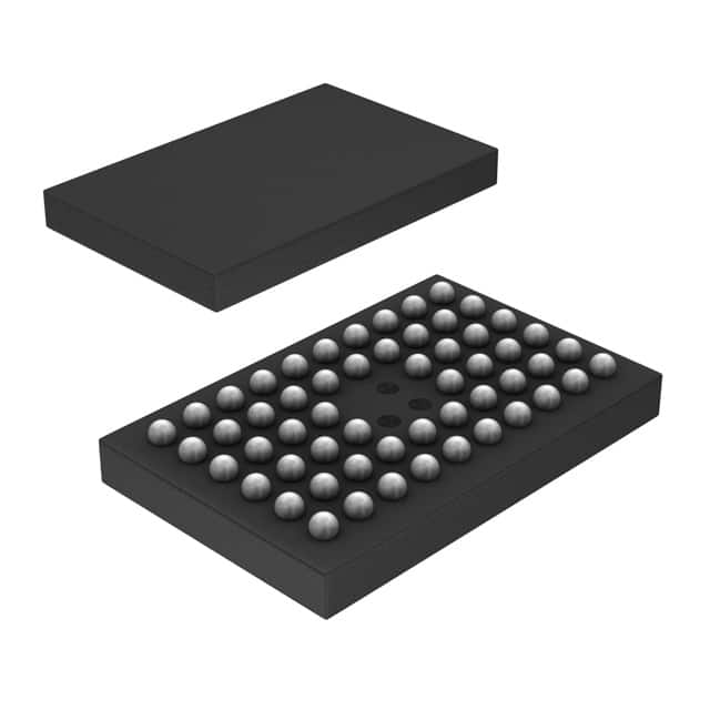
SN74LVCH16245AZQLR
Basic Information Overview
- Category: Integrated Circuit (IC)
- Use: Level Shifting and Signal Conditioning
- Characteristics: Bi-directional voltage level translator with 16-bit wide bus and 3-state outputs
- Package: 48-pin LQFP (Low Profile Quad Flat Package)
- Essence: Translates signals between different voltage domains
- Packaging/Quantity: Tape and Reel, 2500 units per reel
Specifications
- Supply Voltage Range: 1.65V to 3.6V
- Input Voltage Range: 0V to VCC
- Output Voltage Range: 0V to VCC
- Maximum Input Current: ±50mA
- Maximum Output Current: ±32mA
- Operating Temperature Range: -40°C to +85°C
Detailed Pin Configuration
The SN74LVCH16245AZQLR has a total of 48 pins. The pin configuration is as follows:
- OE (Output Enable) 1
- A1 (Data Input/Output) 1
- B1 (Data Input/Output) 1
- GND (Ground)
- B2 (Data Input/Output) 2
- A2 (Data Input/Output) 2
- OE (Output Enable) 2
- VCC (Supply Voltage)
- B3 (Data Input/Output) 3
- A3 (Data Input/Output) 3
- OE (Output Enable) 3
- GND (Ground)
- A4 (Data Input/Output) 4
- B4 (Data Input/Output) 4
- OE (Output Enable) 4
- VCC (Supply Voltage)
- B5 (Data Input/Output) 5
- A5 (Data Input/Output) 5
- OE (Output Enable) 5
- GND (Ground)
- B6 (Data Input/Output) 6
- A6 (Data Input/Output) 6
- OE (Output Enable) 6
- VCC (Supply Voltage)
- B7 (Data Input/Output) 7
- A7 (Data Input/Output) 7
- OE (Output Enable) 7
- GND (Ground)
- A8 (Data Input/Output) 8
- B8 (Data Input/Output) 8
- OE (Output Enable) 8
- VCC (Supply Voltage)
- B9 (Data Input/Output) 9
- A9 (Data Input/Output) 9
- OE (Output Enable) 9
- GND (Ground)
- B10 (Data Input/Output) 10
- A10 (Data Input/Output) 10
- OE (Output Enable) 10
- VCC (Supply Voltage)
- B11 (Data Input/Output) 11
- A11 (Data Input/Output) 11
- OE (Output Enable) 11
- GND (Ground)
- A12 (Data Input/Output) 12
- B12 (Data Input/Output) 12
- OE (Output Enable) 12
- VCC (Supply Voltage)
Functional Features
- Bi-directional voltage level translation between different voltage domains
- 3-state outputs allow multiple devices to share the same bus
- Supports bidirectional data flow with non-inverting outputs
Advantages and Disadvantages
Advantages: - Wide supply voltage range allows compatibility with various systems - High-speed operation for efficient signal translation - 3-state outputs enable bus sharing and reduce the number of required pins
Disadvantages: - Limited maximum input and output current may restrict usage in high-current applications - Temperature range limited to -40°C to +85°C, not suitable for extreme temperature environments
Working Principles
The SN74LVCH16245AZQLR is a voltage level translator that enables communication between devices operating at different voltage levels. It uses a combination of CMOS technology and non-inverting buffers to achieve bidirectional data flow. The OE (Output Enable) pins control the direction of data transmission, allowing the device to function as a translator or as a buffer.
Detailed Application Field Plans
The SN74LVCH16245AZQLR is commonly used in various applications where voltage level shifting and signal conditioning are required. Some specific application fields include: - Communication systems - Industrial automation - Automotive electronics - Consumer electronics - Medical devices
Detailed and Complete Alternative Models
- SN74L
قم بإدراج 10 أسئلة وإجابات شائعة تتعلق بتطبيق SN74LVCH16245AZQLR في الحلول التقنية
Sure! Here are 10 common questions and answers related to the application of SN74LVCH16245AZQLR:
Q: What is SN74LVCH16245AZQLR? A: SN74LVCH16245AZQLR is a 16-bit bus transceiver with 3-state outputs, designed for low-voltage (LV) applications.
Q: What is the voltage range supported by SN74LVCH16245AZQLR? A: SN74LVCH16245AZQLR supports a voltage range of 1.65V to 3.6V.
Q: What is the maximum data transfer rate of SN74LVCH16245AZQLR? A: SN74LVCH16245AZQLR has a maximum data transfer rate of 400 Mbps.
Q: Can SN74LVCH16245AZQLR be used for bidirectional communication? A: Yes, SN74LVCH16245AZQLR can be used for bidirectional communication as it has separate input and output ports.
Q: How many channels does SN74LVCH16245AZQLR have? A: SN74LVCH16245AZQLR has 16 channels, allowing for the transmission of 16 bits simultaneously.
Q: What is the purpose of the 3-state outputs in SN74LVCH16245AZQLR? A: The 3-state outputs allow the user to disable the outputs, effectively disconnecting them from the bus.
Q: Can SN74LVCH16245AZQLR handle level shifting between different voltage domains? A: Yes, SN74LVCH16245AZQLR can be used for level shifting between different voltage domains, making it suitable for interfacing between different logic families.
Q: What is the power supply voltage required for SN74LVCH16245AZQLR? A: SN74LVCH16245AZQLR requires a power supply voltage of 1.65V to 3.6V.
Q: Does SN74LVCH16245AZQLR have any built-in protection features? A: Yes, SN74LVCH16245AZQLR has built-in ESD (electrostatic discharge) protection on all inputs and outputs.
Q: Can SN74LVCH16245AZQLR be used in high-speed applications? A: While SN74LVCH16245AZQLR has a maximum data transfer rate of 400 Mbps, it may not be suitable for very high-speed applications. It is recommended to consult the datasheet for specific application requirements.
Please note that these answers are general and should be verified with the official documentation and datasheet of SN74LVCH16245AZQLR for accurate information.


