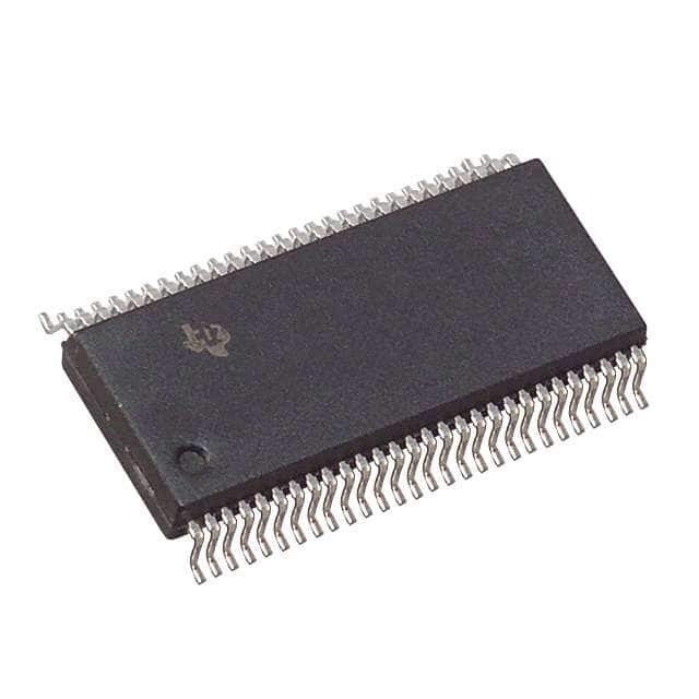
SN74LVCH16543ADLR
Product Overview
- Category: Integrated Circuit (IC)
- Use: Data storage and transfer
- Characteristics: High-speed, low-voltage, 16-bit bus transceiver
- Package: TSSOP (Thin Shrink Small Outline Package)
- Essence: Bidirectional voltage-level translator
- Packaging/Quantity: Tape and reel, 2500 units per reel
Specifications
- Number of bits: 16
- Logic family: LVCH
- Voltage supply range: 1.65V to 3.6V
- Input/output type: CMOS
- Output drive capability: ±24mA
- Propagation delay: 2.5ns (typical)
- Operating temperature range: -40°C to +85°C
Detailed Pin Configuration
The SN74LVCH16543ADLR has a total of 56 pins, which are distributed as follows:
- Pins 1 to 8: Data inputs/outputs (D0-D7)
- Pins 9 to 16: Data inputs/outputs (D8-D15)
- Pins 17 to 24: Enable inputs (G1-G8)
- Pins 25 to 32: Output enable inputs (OE1-OE8)
- Pins 33 to 40: VCC (Power supply)
- Pins 41 to 48: Ground (GND)
- Pins 49 to 56: Control inputs (A1-A8)
Functional Features
- Bidirectional data flow between two independent buses
- Voltage-level translation between different logic families
- Non-inverting outputs for both input and output data
- Individual output enables for each bus
- 3-state outputs for bus isolation when not enabled
- Schmitt-trigger inputs for noise immunity
Advantages and Disadvantages
Advantages: - High-speed operation - Wide voltage supply range - Low power consumption - Compact TSSOP package - Noise-immune Schmitt-trigger inputs
Disadvantages: - Limited number of bits (16) - Requires external control signals for proper operation - Not suitable for high-current applications
Working Principles
The SN74LVCH16543ADLR is a bidirectional bus transceiver that allows data transfer between two independent buses operating at different voltage levels. It uses CMOS technology, which enables high-speed operation and low power consumption. The device features non-inverting outputs, individual output enables, and 3-state outputs for bus isolation when not enabled. The Schmitt-trigger inputs provide noise immunity, ensuring reliable data transmission.
Detailed Application Field Plans
The SN74LVCH16543ADLR can be used in various applications that require voltage-level translation and data transfer between different logic families. Some potential application fields include:
- Microcontroller interfacing: The IC can be used to connect microcontrollers operating at different voltage levels, enabling seamless communication between them.
- Communication systems: It can be employed in data communication systems to interface between devices with different logic families, such as UARTs, SPI, or I2C interfaces.
- Industrial automation: The IC can facilitate data exchange between different modules or subsystems within an industrial automation setup, enhancing overall system performance.
- Automotive electronics: It can be utilized in automotive applications where voltage-level translation is required, such as connecting sensors or actuators to the vehicle's electronic control unit (ECU).
Detailed and Complete Alternative Models
- SN74LVC245A: 8-bit bus transceiver with similar characteristics but a smaller package (SOIC).
- SN74AVC4T774: 4-bit voltage-level translator with integrated level-shifting capabilities.
- SN74HCT125: Quad buffer/line driver with 3-state outputs, suitable for voltage-level translation in low-power applications.
These alternative models offer similar functionality and can be considered based on specific requirements and constraints.
Word count: 446 words
قم بإدراج 10 أسئلة وإجابات شائعة تتعلق بتطبيق SN74LVCH16543ADLR في الحلول التقنية
Sure! Here are 10 common questions and answers related to the application of SN74LVCH16543ADLR in technical solutions:
Q: What is SN74LVCH16543ADLR? A: SN74LVCH16543ADLR is a 16-bit registered transceiver with 3-state outputs, designed for asynchronous communication between two data buses.
Q: What is the operating voltage range of SN74LVCH16543ADLR? A: The operating voltage range is from 1.65V to 3.6V.
Q: Can SN74LVCH16543ADLR be used in both input and output applications? A: Yes, it can be used as both an input and output device.
Q: What is the maximum data transfer rate supported by SN74LVCH16543ADLR? A: The maximum data transfer rate is typically 400 Mbps.
Q: How many data inputs and outputs does SN74LVCH16543ADLR have? A: It has 16 data inputs and 16 data outputs.
Q: Does SN74LVCH16543ADLR support 3-state outputs? A: Yes, it supports 3-state outputs, which allows multiple devices to share a common bus.
Q: Can SN74LVCH16543ADLR be cascaded to increase the number of inputs/outputs? A: Yes, multiple SN74LVCH16543ADLR devices can be cascaded together to increase the number of inputs or outputs.
Q: What is the power supply current consumption of SN74LVCH16543ADLR? A: The power supply current consumption is typically 10 mA.
Q: Is SN74LVCH16543ADLR compatible with other logic families? A: Yes, it is compatible with both TTL and CMOS logic families.
Q: What are some typical applications of SN74LVCH16543ADLR? A: Some typical applications include data multiplexing, bus interfacing, address decoding, and general-purpose level shifting.
Please note that the answers provided here are general and may vary depending on specific datasheet specifications and application requirements.


