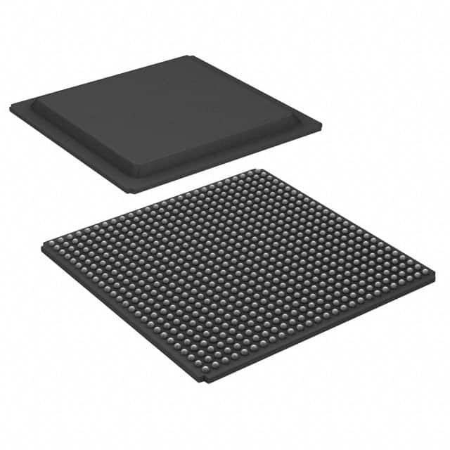
XC6SLX100-N3FG676I
Basic Information Overview
- Category: Integrated Circuit (IC)
- Use: Programmable Logic Device (PLD)
- Characteristics:
- High-performance FPGA (Field-Programmable Gate Array)
- Low-power consumption
- Large capacity
- Advanced features for system integration
- Package: FG676 (Fine-Pitch Ball Grid Array)
- Essence: The XC6SLX100-N3FG676I is a high-performance FPGA designed for various applications that require programmable logic capabilities.
- Packaging/Quantity: Typically sold in reels or trays, with quantities varying based on customer requirements.
Specifications
- Logic Cells: 101,440
- Slices: 15,360
- Flip-Flops: 60,160
- Block RAM: 4,860 Kbits
- DSP Slices: 240
- Maximum Operating Frequency: 550 MHz
- I/O Pins: 500
- Voltage Range: 1.14V to 1.26V
- Operating Temperature Range: -40°C to +100°C
Detailed Pin Configuration
The XC6SLX100-N3FG676I has 676 pins arranged in a Fine-Pitch Ball Grid Array package. Each pin serves a specific purpose, including input, output, power supply, and configuration. A detailed pinout diagram can be found in the device datasheet.
Functional Features
- High-performance FPGA architecture allows for complex digital designs.
- Flexible and reprogrammable nature enables rapid prototyping and design iterations.
- Low-power consumption makes it suitable for battery-powered applications.
- Large capacity provides ample resources for implementing complex algorithms and systems.
- Advanced features such as integrated DSP slices enhance signal processing capabilities.
Advantages
- Versatility: The XC6SLX100-N3FG676I can be programmed to perform a wide range of functions, making it suitable for diverse applications.
- High Performance: With its large number of logic cells and high operating frequency, the FPGA delivers excellent performance for demanding tasks.
- System Integration: The advanced features enable seamless integration with other system components, simplifying overall design complexity.
Disadvantages
- Complexity: Utilizing the full potential of the XC6SLX100-N3FG676I requires expertise in FPGA programming and design.
- Cost: FPGAs can be more expensive compared to other integrated circuits due to their programmable nature.
Working Principles
The XC6SLX100-N3FG676I operates based on the principles of reconfigurable digital logic. It consists of an array of configurable logic blocks interconnected through programmable routing resources. These resources allow users to define the desired functionality by configuring the interconnections and behavior of the logic elements within the FPGA.
Detailed Application Field Plans
The XC6SLX100-N3FG676I finds applications in various fields, including: 1. Communications: Used in wireless base stations, network routers, and data communication equipment. 2. Industrial Automation: Enables control systems for robotics, motor drives, and factory automation. 3. Aerospace and Defense: Utilized in radar systems, avionics, and secure communication devices. 4. Medical Equipment: Supports medical imaging, patient monitoring, and diagnostic instruments. 5. Automotive: Used in automotive electronics for engine control, infotainment systems, and driver assistance.
Detailed and Complete Alternative Models
- XC6SLX75-N3FGG484C
- XC6SLX150-N3FG900I
- XC6SLX25-N3CSG324I
- XC6SLX45-N3CSG324C
- XC6SLX100-N3CSG484I
These alternative models offer different capacities, pin configurations, and package options to cater to specific design requirements.
Word count: 533 words
قم بإدراج 10 أسئلة وإجابات شائعة تتعلق بتطبيق XC6SLX100-N3FG676I في الحلول التقنية
Sure! Here are 10 common questions and answers related to the application of XC6SLX100-N3FG676I in technical solutions:
Question: What is XC6SLX100-N3FG676I?
- Answer: XC6SLX100-N3FG676I is a field-programmable gate array (FPGA) from Xilinx, which offers high-performance processing capabilities for various technical applications.Question: What are the key features of XC6SLX100-N3FG676I?
- Answer: Some key features of XC6SLX100-N3FG676I include a large number of logic cells, high-speed I/O interfaces, embedded memory blocks, and advanced DSP capabilities.Question: What are some typical applications of XC6SLX100-N3FG676I?
- Answer: XC6SLX100-N3FG676I can be used in a wide range of applications such as telecommunications, industrial automation, aerospace, defense, medical devices, and scientific research.Question: How can XC6SLX100-N3FG676I be programmed?
- Answer: XC6SLX100-N3FG676I can be programmed using Xilinx's Vivado Design Suite or ISE Design Suite software tools, which provide a graphical interface for designing and implementing FPGA-based solutions.Question: What is the power consumption of XC6SLX100-N3FG676I?
- Answer: The power consumption of XC6SLX100-N3FG676I depends on the specific design and operating conditions. It is recommended to refer to the datasheet for detailed power consumption information.Question: Can XC6SLX100-N3FG676I interface with other components or devices?
- Answer: Yes, XC6SLX100-N3FG676I supports various standard interfaces such as PCIe, Ethernet, USB, SPI, I2C, and UART, allowing it to communicate with other components or devices in a system.Question: What is the maximum operating frequency of XC6SLX100-N3FG676I?
- Answer: The maximum operating frequency of XC6SLX100-N3FG676I depends on the specific design and implementation. It is recommended to refer to the datasheet for detailed timing information.Question: Can XC6SLX100-N3FG676I be used in safety-critical applications?
- Answer: Yes, XC6SLX100-N3FG676I can be used in safety-critical applications. However, it is important to follow appropriate design practices and consider additional safety measures to ensure reliable operation.Question: Are there any development boards available for XC6SLX100-N3FG676I?
- Answer: Yes, Xilinx offers development boards such as the Spartan-6 FPGA SP601 Evaluation Kit, which can be used for prototyping and testing designs based on XC6SLX100-N3FG676I.Question: Where can I find more resources and support for XC6SLX100-N3FG676I?
- Answer: You can find more resources, documentation, and support for XC6SLX100-N3FG676I on Xilinx's official website, including user guides, application notes, forums, and technical support channels.


